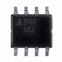
CA3140AMZ Intersil, CA3140AMZ Datasheet - Page 9

CA3140AMZ
Manufacturer Part Number
CA3140AMZ
Description
IC OPAMP BIMOS 4.5MHZ 8SOIC
Manufacturer
Intersil
Datasheet
1.CA3140AEZ.pdf
(23 pages)
Specifications of CA3140AMZ
Amplifier Type
General Purpose
Number Of Circuits
1
Slew Rate
9 V/µs
Gain Bandwidth Product
4.5MHz
Current - Input Bias
10pA
Voltage - Input Offset
2000µV
Current - Supply
4mA
Current - Output / Channel
40mA
Voltage - Supply, Single/dual (±)
4 V ~ 36 V, ±2 V ~ 18 V
Operating Temperature
-55°C ~ 125°C
Mounting Type
Surface Mount
Package / Case
8-SOIC (3.9mm Width)
Lead Free Status / RoHS Status
Lead free / RoHS Compliant
Output Type
-
-3db Bandwidth
-
Available stocks
Company
Part Number
Manufacturer
Quantity
Price
Part Number:
CA3140AMZ
Manufacturer:
INTERSIL
Quantity:
20 000
Company:
Part Number:
CA3140AMZ96
Manufacturer:
DDC
Quantity:
11
Part Number:
CA3140AMZ96
Manufacturer:
INTERSIL
Quantity:
20 000
the CA3140 is used as a unity gain voltage follower. This
resistance prevents the possibility of extremely large input
signal transients from forcing a signal through the input
protection network and directly driving the internal constant
current source which could result in positive feedback via the
output terminal. A 3.9kΩ resistor is sufficient.
The typical input current is on the order of 10pA when the
inputs are centered at nominal device dissipation. As the
output supplies load current, device dissipation will increase,
raising the chip temperature and resulting in increased input
current. Figure 7 shows typical input terminal current versus
ambient temperature for the CA3140.
It is well known that MOSFET devices can exhibit slight
changes in characteristics (for example, small changes in
FIGURE 6. OPEN LOOP VOLTAGE GAIN AND PHASE vs
100
80
60
40
20
0
10
-0.5
-1.0
-1.5
-2.0
-2.5
-3.0
SUPPLY VOLTAGE: V
T
1
A
FIGURE 8. OUTPUT VOLTAGE SWING CAPABILITY AND COMMON MODE INPUT VOLTAGE RANGE vs SUPPLY VOLTAGE
0
= 25
0
R
10
+V
+V
+V
L
o
FREQUENCY
2
ICR
C
=
ICR
ICR
∞
AT T
AT T
AT T
10
5
3
A
A
A
FREQUENCY (Hz)
= 125
= -55
= 25
SUPPLY VOLTAGE (V+, V-)
S
10
= ±15V
4
o
o
o
C
C
C
10
9
R
C
10
L
L
5
= 2kΩ,
= 100pF
φOL
10
15
6
+V
+V
+V
R
C
OUT
OUT
OUT
L
L
10
= 2kΩ,
= 0pF
7
AT T
AT T
AT T
20
A
A
A
10
= 125
= 25
= -55
CA3140, CA3140A
-75
-90
-105
-120
-135
-150
8
o
o
o
C
C
C
25
input offset voltage) due to the application of large
differential input voltages that are sustained over long
periods at elevated temperatures.
Both applied voltage and temperature accelerate these
changes. The process is reversible and offset voltage shifts of
the opposite polarity reverse the offset. Figure 9 shows the
typical offset voltage change as a function of various stress
voltages at the maximum rating of 125
lower temperatures (metal can and plastic), for example, at
85
linear applications, where the differential voltage is small and
symmetrical, these incremental changes are of about the
same magnitude as those encountered in an operational
amplifier employing a bipolar transistor input stage.
o
C, this change in voltage is considerably less. In typical
10K
100
-0.5
-1.0
-1.5
1K
10
1.5
1.0
0.5
1
FIGURE 7. INPUT CURRENT vs TEMPERATURE
-60
0
0
SUPPLY VOLTAGE: V
-40
-V
T
A
OUT
= -55
-20
FOR
5
o
C to 125
0
SUPPLY VOLTAGE (V+, V-)
TEMPERATURE (
o
C
S
20
10
= ±15V
40
o
60
15
C (for metal can); at
o
-V
-V
-V
C)
ICR
ICR
ICR
80
AT T
AT T
AT T
100
20
A
A
A
= 125
= 25
= -55
July 11, 2005
120
FN957.10
o
o
o
C
C
C
140
25


