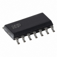
SA5211D/01,112 NXP Semiconductors, SA5211D/01,112 Datasheet - Page 13

SA5211D/01,112
Manufacturer Part Number
SA5211D/01,112
Description
IC TRANSIMP AMP 180MHZ 14-SOIC
Manufacturer
NXP Semiconductors
Datasheet
1.SA5211D602.pdf
(29 pages)
Specifications of SA5211D/01,112
Amplifier Type
Transimpedance
Number Of Circuits
1
Output Type
Differential
-3db Bandwidth
180MHz
Current - Supply
26mA
Current - Output / Channel
4mA
Voltage - Supply, Single/dual (±)
4.5 V ~ 5.5 V
Operating Temperature
-40°C ~ 85°C
Mounting Type
Surface Mount
Package / Case
14-SOIC (3.9mm Width), 14-SOL
Lead Free Status / RoHS Status
Lead free / RoHS Compliant
Slew Rate
-
Gain Bandwidth Product
-
Current - Input Bias
-
Voltage - Input Offset
-
Other names
568-2449-5
935275219112
SA5211D/01
935275219112
SA5211D/01
11. Theory of operation
Philips Semiconductors
9397 750 07427
Product specification
Fig 10. Typical performance characteristics. (cont.)
Transimpedance amplifiers have been widely used as the preamplifier in fiber-optic
receivers. The SA5211 is a wide bandwidth (typically 180 MHz) transimpedance
amplifier designed primarily for input currents requiring a large dynamic range, such
as those produced by a laser diode. The maximum input current before output stage
clipping occurs at typically 50 A. The SA5211 is a bipolar transimpedance amplifier
which is current driven at the input and generates a differential voltage signal at the
outputs. The forward transfer function is therefore a ratio of the differential output
voltage to a given input current with the dimensions of ohms. The main feature of this
amplifier is a wideband, low-noise input stage which is desensitized to photodiode
capacitance variations. When connected to a photodiode of a few picoFarads, the
frequency response will not be degraded significantly. Except for the input stage, the
entire signal path is differential to provide improved power-supply rejection and ease
of interface to ECL type circuitry. A block diagram of the circuit is shown in
The input stage (A1) employs shunt-series feedback to stabilize the current gain of
the amplifier. The transresistance of the amplifier from the current source to the
emitter of Q
gain from the second stage (A2) and emitter followers (A3 and A4) is about two.
Therefore, the differential transresistance of the entire amplifier, R
The single-ended transresistance of the amplifier is typically 14.4 k .
The simplified schematic in
differential output voltage. The amplifier has a single input for current which is
referenced to Ground 1. An input current from a laser diode, for example, will be
converted into a voltage by the feedback resistor R
of the open loop gain of the circuit, A
loading on Q
interface with the Q
an internal reference, V
R
T
=
V
---------------------------- -
OUT
I
IN
3
1
diff
is approximately the value of the feedback resistor, R
. The transistor Q
Rev. 03 — 07 October 1998
=
Output Step Response
15
2 R
– Q
B2
F
16
. The differential outputs are derived from emitter followers
=
Figure 12
differential pair of the second stage which is biased with
2 14.4 K
4
, resistor R
VOL
shows how an input current is converted to a
=
70. The emitter follower Q
28.8 k
7
, and V
Transimpedance amplifier (180 MHz)
F
. The transistor Q1 provides most
B1
provide level shifting and
°
© Philips Electronics N.V. 2001. All rights reserved.
T
F
2
is
= 14.4 k . The
SA5211
minimizes
Figure
13 of 28
11.
(1)


