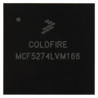
MCF5274LVM166 Freescale Semiconductor, MCF5274LVM166 Datasheet - Page 12

MCF5274LVM166
Manufacturer Part Number
MCF5274LVM166
Description
IC MPU 32BIT COLDF 196-MAPBGA
Manufacturer
Freescale Semiconductor
Series
MCF527xr
Datasheet
1.MCF5274LVM166J.pdf
(44 pages)
Specifications of MCF5274LVM166
Core Processor
Coldfire V2
Core Size
32-Bit
Speed
166MHz
Connectivity
EBI/EMI, Ethernet, I²C, SPI, UART/USART, USB
Peripherals
DMA, WDT
Number Of I /o
61
Program Memory Type
ROMless
Ram Size
64K x 8
Voltage - Supply (vcc/vdd)
1.4 V ~ 1.6 V
Oscillator Type
External
Operating Temperature
0°C ~ 70°C
Package / Case
196-MAPBGA
Embedded Interface Type
I2C, SPI, USB, UART
Digital Ic Case Style
BGA
No. Of Pins
196
Operating Temperature Range
0°C To +70°C
Frequency Typ
166MHz
Rohs Compliant
Yes
Family Name
MCF5xxx
Device Core
ColdFire
Device Core Size
32b
Frequency (max)
166MHz
Instruction Set Architecture
RISC
Operating Supply Voltage (max)
1.6V
Operating Supply Voltage (min)
1.4V
Operating Temp Range
0C to 70C
Operating Temperature Classification
Commercial
Mounting
Surface Mount
Pin Count
196
Package Type
MA-BGA
Lead Free Status / RoHS Status
Lead free / RoHS Compliant
Eeprom Size
-
Program Memory Size
-
Data Converters
-
Lead Free Status / Rohs Status
Compliant
Available stocks
Company
Part Number
Manufacturer
Quantity
Price
Company:
Part Number:
MCF5274LVM166
Manufacturer:
FREESCALE
Quantity:
201
Company:
Part Number:
MCF5274LVM166
Manufacturer:
Freescale Semiconductor
Quantity:
10 000
Company:
Part Number:
MCF5274LVM166J
Manufacturer:
Freescale Semiconductor
Quantity:
10 000
Design Recommendations
5.7
5.7.1
5.7.1.1
Table 3
5.7.1.2
See the SDRAM controller module chapter in the MCF5275 Reference Manual for details on address
multiplexing.
5.7.2
The FEC supports an MII interface for 10/100 Mbps Ethernet and a seven-wire serial interface for 10 Mbps
Ethernet. The interface mode is selected by R_CNTRL[MII_MODE]. In MII mode, the 802.3 standard
defines and the FEC module supports 18 signals. These are shown in
12
DDR_CLKOUT Bus clock output. Connects to the CLK input of SDRAMs.
shows the behavior of SDRAM signals in synchronous mode.
SD_CS[1:0]
SD_SRAS
SD_SCAS
SD_CKE
Interface Recommendations
SD_WE
BS[3:2]
Signal
DDR SDRAM Controller
Ethernet PHY Transceiver Connection
SDRAM Controller Signals in Synchronous Mode
Address Multiplexing
MCF5275 Integrated Microprocessor Family Hardware Specification, Rev. 4
Synchronous row address strobe. Indicates a valid SDRAM row address is present and can be
latched by the SDRAM. SD_SRAS should be connected to the corresponding SDRAM
SD_SRAS. Do not confuse SD_SRAS with the DRAM controller’s SDRAM_CS[1:0], which
should not be interfaced to the SDRAM SD_SRAS signals.
Synchronous column address strobe. Indicates a valid column address is present and can be
latched by the SDRAM. SD_SCAS should be connected to the corresponding signal labeled
SD_SCAS on the SDRAM.
DRAM read/write. Asserted for write operations and negated for read operations.
Row address strobe. Select each memory block of SDRAMs connected to the MCF5275. One
SDRAM_CS signal selects one SDRAM block and connects to the corresponding CS signals.
Synchronous DRAM clock enable. Connected directly to the CKE (clock enable) signal of
SDRAMs. Enables and disables the clock internal to SDRAM. When CKE is low, memory can
enter a power-down mode where operations are suspended or they can enter self-refresh
mode. SD_CKE functionality is controlled by DCR[COC]. For designs using external
multiplexing, setting COC allows SD_CKE to provide command-bit functionality.
Column address strobe. For synchronous operation, BS[3:2] function as byte enables to the
SDRAMs. They connect to the DQM signals (or mask qualifiers) of the SDRAMs.
Transmit clock
Transmit enable
Transmit data
Transmit error
Table 3. Synchronous DRAM Signal Connections
Signal Description
Table 4. MII Mode
Description
FECn_TXCLK
FECn_TXEN
FECn_TXD[3:0]
FECn_TXER
MCF5275 Pin
Table
4.
Freescale Semiconductor


