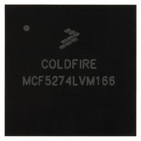
MCF5274LVM166 Freescale Semiconductor, MCF5274LVM166 Datasheet - Page 40

MCF5274LVM166
Manufacturer Part Number
MCF5274LVM166
Description
IC MPU 32BIT COLDF 196-MAPBGA
Manufacturer
Freescale Semiconductor
Series
MCF527xr
Datasheet
1.MCF5274LVM166J.pdf
(44 pages)
Specifications of MCF5274LVM166
Core Processor
Coldfire V2
Core Size
32-Bit
Speed
166MHz
Connectivity
EBI/EMI, Ethernet, I²C, SPI, UART/USART, USB
Peripherals
DMA, WDT
Number Of I /o
61
Program Memory Type
ROMless
Ram Size
64K x 8
Voltage - Supply (vcc/vdd)
1.4 V ~ 1.6 V
Oscillator Type
External
Operating Temperature
0°C ~ 70°C
Package / Case
196-MAPBGA
Embedded Interface Type
I2C, SPI, USB, UART
Digital Ic Case Style
BGA
No. Of Pins
196
Operating Temperature Range
0°C To +70°C
Frequency Typ
166MHz
Rohs Compliant
Yes
Family Name
MCF5xxx
Device Core
ColdFire
Device Core Size
32b
Frequency (max)
166MHz
Instruction Set Architecture
RISC
Operating Supply Voltage (max)
1.6V
Operating Supply Voltage (min)
1.4V
Operating Temp Range
0C to 70C
Operating Temperature Classification
Commercial
Mounting
Surface Mount
Pin Count
196
Package Type
MA-BGA
Lead Free Status / RoHS Status
Lead free / RoHS Compliant
Eeprom Size
-
Program Memory Size
-
Data Converters
-
Lead Free Status / Rohs Status
Compliant
Available stocks
Company
Part Number
Manufacturer
Quantity
Price
Company:
Part Number:
MCF5274LVM166
Manufacturer:
FREESCALE
Quantity:
201
Company:
Part Number:
MCF5274LVM166
Manufacturer:
Freescale Semiconductor
Quantity:
10 000
Company:
Part Number:
MCF5274LVM166J
Manufacturer:
Freescale Semiconductor
Quantity:
10 000
Electrical Characteristics
8.15
40
1
Num
J10
J11
J12
J13
J14
JTAG_EN is expected to be a static signal. Hence, it is not associated with any timing.
J1
J2
J3
J4
J5
J6
J7
J8
J9
QSPI_CS[3:0]
QSPI_DOUT
QSPI_CLK
QSPI_DIN
TCLK Frequency of Operation
TCLK Cycle Period
TCLK Clock Pulse Width
TCLK Rise and Fall Times
Boundary Scan Input Data Setup Time to TCLK Rise
Boundary Scan Input Data Hold Time after TCLK Rise
TCLK Low to Boundary Scan Output Data Valid
TCLK Low to Boundary Scan Output High Z
TMS, TDI Input Data Setup Time to TCLK Rise
TMS, TDI Input Data Hold Time after TCLK Rise
TCLK Low to TDO Data Valid
TCLK Low to TDO High Z
TRST Assert Time
TRST Setup Time (Negation) to TCLK High
JTAG and Boundary Scan Timing
MCF5275 Integrated Microprocessor Family Hardware Specification, Rev. 4
QS3
Characteristics
QS1
Table 27. JTAG and Boundary Scan Timing
QS2
Figure 22. QSPI Timing
1
Symbol
t
t
t
t
t
t
t
t
TAPBST
TAPBHT
TRSTST
TRSTAT
TDODZ
f
t
BSDST
BSDHT
t
t
TDODV
t
t
JCYC
JCYC
BSDV
BSDZ
JCRF
JCW
QS4
4 x t
Min
100
DC
26
26
10
10
0
4
0
0
4
0
0
CYC
QS5
Freescale Semiconductor
Max
1/4
33
33
26
—
—
—
—
—
—
—
—
3
8
f
Unit
sys/2
ns
ns
ns
ns
ns
ns
ns
ns
ns
ns
ns
ns
ns


