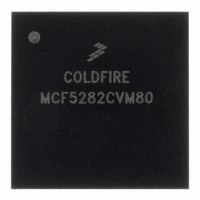
MCF5282CVM80 Freescale Semiconductor, MCF5282CVM80 Datasheet - Page 332

MCF5282CVM80
Manufacturer Part Number
MCF5282CVM80
Description
IC MPU 512K 80MHZ 256-MAPBGA
Manufacturer
Freescale Semiconductor
Series
MCF528xr
Datasheet
1.MCF5216CVM66J.pdf
(766 pages)
Specifications of MCF5282CVM80
Core Processor
Coldfire V2
Core Size
32-Bit
Speed
80MHz
Connectivity
CAN, EBI/EMI, Ethernet, I²C, SPI, UART/USART
Peripherals
DMA, LVD, POR, PWM, WDT
Number Of I /o
150
Program Memory Size
512KB (512K x 8)
Program Memory Type
FLASH
Ram Size
64K x 8
Voltage - Supply (vcc/vdd)
2.7 V ~ 3.6 V
Data Converters
A/D 8x10b
Oscillator Type
External
Operating Temperature
-40°C ~ 85°C
Package / Case
256-MAPBGA
Controller Family/series
ColdFire
Ram Memory Size
64KB
Embedded Interface Type
CAN, I2C, SPI, UART
No. Of Pwm Channels
8
Digital Ic Case Style
MAPBGA
Rohs Compliant
Yes
Lead Free Status / RoHS Status
Lead free / RoHS Compliant
Eeprom Size
-
Available stocks
Company
Part Number
Manufacturer
Quantity
Price
Company:
Part Number:
MCF5282CVM80
Manufacturer:
FREESCALE
Quantity:
1 831
Company:
Part Number:
MCF5282CVM80
Manufacturer:
Freescale Semiconductor
Quantity:
10 000
Company:
Part Number:
MCF5282CVM80J
Manufacturer:
Freescale Semiconductor
Quantity:
10 000
- Current page: 332 of 766
- Download datasheet (9Mb)
Fast Ethernet Controller (FEC)
17.4.19 Transmit FIFO Watermark Register (TFWR)
The TFWR controls the amount of data required in the transmit FIFO before transmission of a frame can
begin. This allows you to minimize transmit latency (TFWR = 00 or 01) or allow for larger bus access
latency (TFWR = 11) due to contention for the system bus. Setting the watermark to a high value
minimizes the risk of transmit FIFO underrun due to contention for the system bus. The byte counts
associated with the TFWR field may need to be modified to match a given system requirement (worst case
bus access latency by the transmit data DMA channel).
17.4.20 FIFO Receive Bound Register (FRBR)
FRBR indicates the upper address bound of the FIFO RAM. Drivers can use this value, along with the
FRSR, to appropriately divide the available FIFO RAM between the transmit and receive data paths.
17-22
GADDR2
TFWR
Field
Field
31–0
31–2
1–0
IPSBAR
IPSBAR
Offset:
Offset:
Reset 0 0 0 0 0 0 0 0 0 0 0 0 0 0 0 0 0 0 0 0 0 0 0 0 0 0 0 0 0 0 0
Reset 0 0 0 0 0 0 0 0 0 0 0 0 0 0 0 0 0 0 0 0 0 1 1 0 0 0 0 0 0 0 0
The GADDR2 register contains the lower 32 bits of the 64-bit hash table used in the address recognition process for
receive frames with a multicast address. Bit 31 of GADDR2 contains hash index bit 31. Bit 0 of GADDR2 contains
hash index bit 0.
Reserved, must be cleared.
Number of bytes written to transmit FIFO before transmission of a frame begins
00 64 bytes written
01 64 bytes written
10 128 bytes written
11 192 bytes written
W
W
R 0 0 0 0 0 0 0 0 0 0 0 0 0 0 0 0 0 0 0 0 0 0 0 0 0 0 0 0 0 0
R 0 0 0 0 0 0 0 0 0 0 0 0 0 0 0 0 0 0 0 0 0 1
0x1144
0x114C
31 30 29 28 27 26 25 24 23 22 21 20 19 18 17 16 15 14 13 12 11 10 9
31 30 29 28 27 26 25 24 23 22 21 20 19 18 17 16 15 14 13 12 11 10 9
Figure 17-19. Transmit FIFO Watermark Register (TFWR)
MCF5282 and MCF5216 ColdFire Microcontroller User’s Manual, Rev. 3
Figure 17-20. FIFO Receive Bound Register (FRBR)
Table 17-23. TFWR Field Descriptions
Table 17-22. GALR Field Descriptions
Description
Description
8
8
R_BOUND
7
7
Access: User read/write
Access: User read-only
6
6
Freescale Semiconductor
5
5
4
4
3
3
2
2
TFWR
0
1
1
0
0
0
0
0
Related parts for MCF5282CVM80
Image
Part Number
Description
Manufacturer
Datasheet
Request
R
Part Number:
Description:
Mcf5282 And Mcf5216 Coldfire Microcontroller User�s Manual
Manufacturer:
Freescale Semiconductor, Inc
Datasheet:
Part Number:
Description:
Manufacturer:
Freescale Semiconductor, Inc
Datasheet:
Part Number:
Description:
Manufacturer:
Freescale Semiconductor, Inc
Datasheet:
Part Number:
Description:
Manufacturer:
Freescale Semiconductor, Inc
Datasheet:
Part Number:
Description:
Manufacturer:
Freescale Semiconductor, Inc
Datasheet:
Part Number:
Description:
Manufacturer:
Freescale Semiconductor, Inc
Datasheet:
Part Number:
Description:
Manufacturer:
Freescale Semiconductor, Inc
Datasheet:
Part Number:
Description:
Manufacturer:
Freescale Semiconductor, Inc
Datasheet:
Part Number:
Description:
Manufacturer:
Freescale Semiconductor, Inc
Datasheet:
Part Number:
Description:
Manufacturer:
Freescale Semiconductor, Inc
Datasheet:
Part Number:
Description:
Manufacturer:
Freescale Semiconductor, Inc
Datasheet:
Part Number:
Description:
Manufacturer:
Freescale Semiconductor, Inc
Datasheet:
Part Number:
Description:
Manufacturer:
Freescale Semiconductor, Inc
Datasheet:
Part Number:
Description:
Manufacturer:
Freescale Semiconductor, Inc
Datasheet:
Part Number:
Description:
Manufacturer:
Freescale Semiconductor, Inc
Datasheet:


