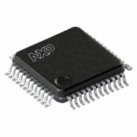
SC16C752BIB48,151 NXP Semiconductors, SC16C752BIB48,151 Datasheet - Page 25

SC16C752BIB48,151
Manufacturer Part Number
SC16C752BIB48,151
Description
IC DUAL UART 64BYTE 48LQFP
Manufacturer
NXP Semiconductors
Datasheet
1.SC16C752BIBS128.pdf
(47 pages)
Specifications of SC16C752BIB48,151
Number Of Channels
2, DUART
Package / Case
48-LFQFP
Fifo's
64 Byte
Voltage - Supply
2.5V, 3.3V, 5V
With Auto Flow Control
Yes
With False Start Bit Detection
Yes
With Modem Control
Yes
Mounting Type
Surface Mount
Voltage
2.25 V ~ 5.5 V
Data Rate
5 Mbps
Supply Voltage (max)
5.5 V
Supply Voltage (min)
2.25 V
Supply Current
4.5 mA
Maximum Operating Temperature
+ 85 C
Minimum Operating Temperature
- 40 C
Mounting Style
SMD/SMT
Operating Supply Voltage
2.5 V or 3.3 V or 5 V
Lead Free Status / RoHS Status
Lead free / RoHS Compliant
Features
-
Lead Free Status / Rohs Status
Lead free / RoHS Compliant
Other names
935274411151
SC16C752BIB48-S
SC16C752BIB48-S
SC16C752BIB48-S
SC16C752BIB48-S
Available stocks
Company
Part Number
Manufacturer
Quantity
Price
Company:
Part Number:
SC16C752BIB48,151
Manufacturer:
NXP Semiconductors
Quantity:
10 000
NXP Semiconductors
SC16C752B
Product data sheet
7.6 Modem Control Register (MCR)
The MCR controls the interface with the mode, data set, or peripheral device that is
emulating the modem.
Table 14.
[1]
Bit
7
6
5
4
3
2
1
0
MCR[7:5] can only be modified when EFR[4] is set, i.e., EFR[4] is a write enable.
MCR[7]
MCR[6]
MCR[5]
MCR[4]
MCR[3]
MCR[2]
MCR[1]
MCR[0]
Symbol
Modem Control Register bits description
[1]
[1]
[1]
All information provided in this document is subject to legal disclaimers.
Description
Clock select.
TCR and TLR enable.
Xon Any.
Enable loopback.
IRQ enable OP.
FIFO Ready enable.
RTS
DTR
5 V, 2.2 V and 2.5 V dual UART, 5 Mbit/s (max.), with 64-byte FIFOs
logic 0 = divide-by-1 clock input
logic 1 = divide-by-4 clock input
logic 0 = no action
logic 1 = enable access to the TCR and TLR registers
logic 0 = disable Xon Any function
logic 1 = enable Xon Any function
logic 0 = normal operating mode.
logic 1 = enable local Loopback mode (internal). In this mode the MCR[3:0]
signals are looped back into MSR[7:4] and the TXn output is looped back to
the RXn input internally.
logic 0 = forces INTA, INTB outputs to the 3-state mode and OP output to
HIGH state
logic 1 = forces the INTA-INTB outputs to the active state and OP output to
LOW state. In Loopback mode, controls MSR[7].
logic 0 = disable the FIFO Rdy register
logic 1 = enable the FIFO Rdy register. In Loopback mode, controls MSR[6].
logic 0 = force RTSn output to inactive (HIGH)
logic 1 = force RTSn output to active (LOW). In loopback mode, controls
MSR[4]. If auto-RTS is enabled, the RTSn output is controlled by hardware
flow control.
logic 0 = force DTRn output to inactive (HIGH)
logic 1 = force DTRn output to active (LOW). In Loopback mode, controls
MSR[5].
Rev. 6 — 30 November 2010
Table 14
shows modem control register bit settings.
SC16C752B
© NXP B.V. 2010. All rights reserved.
25 of 47


