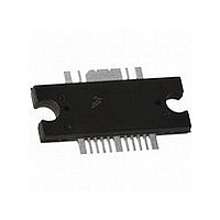
MW7IC2425NBR1 Freescale Semiconductor, MW7IC2425NBR1 Datasheet

MW7IC2425NBR1
Specifications of MW7IC2425NBR1
Related parts for MW7IC2425NBR1
MW7IC2425NBR1 Summary of contents
Page 1
... Freescale Semiconductor, Inc., 2009. All rights reserved. RF Device Data Freescale Semiconductor = 55 mA 195 mA, DQ1 DQ2 Operation out DS2 (1) MW7IC2425NR1 MW7IC2425GNR1 MW7IC2425NBR1 Document Number: MW7IC2425N Rev. 0, 3/2009 MW7IC2425NR1 MW7IC2425GNR1 MW7IC2425NBR1 2450 MHz CW LATERAL N - CHANNEL RF POWER MOSFETs CASE 1886 - 270 PLASTIC MW7IC2425NR1 CASE 1887 - 01 ...
Page 2
... MTTF calculator available at http://www.freescale.com/rf. Select Software & Tools/Development Tools/Calculators to access MTTF calculators by product. 3. Refer to AN1955, Thermal Measurement Methodology of RF Power Amplifiers http://www.freescale.com/rf. Select Documentation/Application Notes - AN1955. 4. Measured in Freescale Narrowband Test Fixture. 5. See Appendix A for functional test measurements and test fixture. MW7IC2425NR1 MW7IC2425GNR1 MW7IC2425NBR1 2 Stage 1, 28 Vdc DQ1 Stage 2, 28 Vdc, I ...
Page 3
... V DS(on) C oss = 0 Vdc) GS (4) (2) (In Freescale Narrowband Test Fixture PAE IRL = 28 Vdc mA DQ1 G ps PAE PAR ACPR IRL MW7IC2425NR1 MW7IC2425GNR1 MW7IC2425NBR1 Min Typ Max — — 10 — — 1 — — 1 1.2 1.9 2.7 — 2.7 — 9.5 10.5 11.5 0.15 0.47 0.8 — ...
Page 4
... Chip Capacitors C2, C5, C8, C13 10 nF Chip Capacitors C3, C6, C9, C14 1 μ Chip Capacitors C10 2.4 pF Chip Capacitor C11 3.3 pF Chip Capacitor C16, C17 10 μ Chip Capacitors R1 KΩ, 1/4 W Chip Resistors R2, R3, R5 KΩ, 1/4 W Chip Resistors MW7IC2425NR1 MW7IC2425GNR1 MW7IC2425NBR1 4 NC DUT ...
Page 5
... Figure 4. MW7IC2425NR1(GNR1)(NBR1) Narrowband Test Circuit Component Layout RF Device Data Freescale Semiconductor C15 C17 C14 C9 C13 C10 MW7IC2425NR1 MW7IC2425GNR1 MW7IC2425NBR1 MW7IC2425N Rev C16 C12 C11 5 ...
Page 6
... Figure 5. Power Gain and Power Added Efficiency versus CW Output Power 0.1 Figure 7. Power Gain and Power Added Efficiency versus CW Output Power as a Function 0.1 Figure 8. Power Gain and Power Added Efficiency versus CW Output Power as a Function of V MW7IC2425NR1 MW7IC2425GNR1 MW7IC2425NBR1 P1dB = 44.5 dBm (28. 100 13 Figure 6 ...
Page 7
... 2450 MHz OUTPUT POWER (WATTS) CW out 1st Stage 2nd Stage 110 130 150 170 190 210 T , JUNCTION TEMPERATURE (° Vdc CW, and PAE = 43.8%. DD out MW7IC2425NR1 MW7IC2425GNR1 MW7IC2425NBR1 50 varied from Vdc 195 mA DQ2 0 100 DQ1 Vdc DQ1 10 100 ...
Page 8
... Z load f = 2450 MHz Figure 12. Series Equivalent Source and Load Impedance — Narrowband MW7IC2425NR1 MW7IC2425GNR1 MW7IC2425NBR1 Ω source f = 2450 MHz Vdc mA 195 mA DQ1 DQ2 out source MHz W 2450 32 - j6.256 6.2 - j1. Test circuit impedance as measured from source gate to ground Test circuit impedance as measured from load drain to ground ...
Page 9
... RF Device Data Freescale Semiconductor PACKAGE DIMENSIONS MW7IC2425NR1 MW7IC2425GNR1 MW7IC2425NBR1 9 ...
Page 10
... MW7IC2425NR1 MW7IC2425GNR1 MW7IC2425NBR1 10 RF Device Data Freescale Semiconductor ...
Page 11
... RF Device Data Freescale Semiconductor MW7IC2425NR1 MW7IC2425GNR1 MW7IC2425NBR1 11 ...
Page 12
... MW7IC2425NR1 MW7IC2425GNR1 MW7IC2425NBR1 12 RF Device Data Freescale Semiconductor ...
Page 13
... RF Device Data Freescale Semiconductor MW7IC2425NR1 MW7IC2425GNR1 MW7IC2425NBR1 13 ...
Page 14
... MW7IC2425NR1 MW7IC2425GNR1 MW7IC2425NBR1 14 RF Device Data Freescale Semiconductor ...
Page 15
... RF Device Data Freescale Semiconductor MW7IC2425NR1 MW7IC2425GNR1 MW7IC2425NBR1 15 ...
Page 16
... MW7IC2425NR1 MW7IC2425GNR1 MW7IC2425NBR1 16 RF Device Data Freescale Semiconductor ...
Page 17
... RF Device Data Freescale Semiconductor MW7IC2425NR1 MW7IC2425GNR1 MW7IC2425NBR1 17 ...
Page 18
... AN3789: Clamping of High Power RF Transistors and RFICs in Over - Molded Plastic Packages Engineering Bulletins • EB212: Using Data Sheet Impedances for RF LDMOS Devices The following table summarizes revisions to this document. Revision Date 0 Mar. 2009 • Initial Release of Data Sheet MW7IC2425NR1 MW7IC2425GNR1 MW7IC2425NBR1 18 PRODUCT DOCUMENTATION REVISION HISTORY Description RF Device Data Freescale Semiconductor ...
Page 19
... Rogers R04350B, 0.0133″, ε * Line length includes microstrip bends = 25°C unless otherwise noted) C Symbol = 28 Vdc mA DQ1 G ps PAE PAR ACPR IRL MW7IC2425NR1 MW7IC2425GNR1 MW7IC2425NBR1 MW7IC2725N Rev. 1.3 B1 C16 C12 C11 = 3.48 r Min Typ Max Unit = 275 mA Avg 2700 MHz, DQ2 out 25 ...
Page 20
... DS DQ2 Fixture Gate Quiescent Voltage ( Vdc 275 mAdc, Measured in Functional Test) DD DQ2 Table 2. Thermal Characteristics Characteristic Thermal Resistance, Junction to Case (Case Temperature 81° CW) out MW7IC2425NR1 MW7IC2425GNR1 MW7IC2425NBR1 20 APPENDIX A (continued) = 25°C unless otherwise noted) C Symbol V GS(Q) V GG(Q) V GS(Q) V GG(Q) Stage 1, 28 Vdc, I ...
Page 21
... Semiconductor was negligent regarding the design or manufacture of the part. Freescalet and the Freescale logo are trademarks of Freescale Semiconductor, Inc. All other product or service names are the property of their respective owners. © Freescale Semiconductor, Inc. 2009. All rights reserved. MW7IC2425NR1 MW7IC2425GNR1 MW7IC2425NBR1 21 ...


