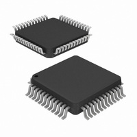
ISL5829INZ Intersil, ISL5829INZ Datasheet - Page 12

ISL5829INZ
Manufacturer Part Number
ISL5829INZ
Description
IC CONV DUAL 12BIT 3.3V 48-LQFP
Manufacturer
Intersil
Datasheet
1.ISL5829EVAL1.pdf
(13 pages)
Specifications of ISL5829INZ
Function
D/A Converter
Rf Type
Cellular, GSM, EDGE, WCDMA
Secondary Attributes
Dual 12-Bit
Package / Case
48-LQFP
Lead Free Status / RoHS Status
Lead free / RoHS Compliant
R
performance of Figure 13 and Figure 14 is basically the
same, however leaving the center tap of Figure 14 floating
allows the circuit to find a more balanced virtual ground,
theoretically improving the even order harmonic rejection,
but likely reducing the signal swing available due to the
output voltage compliance range limitations.
Timing Diagram
A
FIGURE 13. OUTPUT LOADING FOR DATASHEET
R
ISL5829
=R
EQ
AT EACH OUTPUT
B
= 0.5 x (R
=50Ω, R
D11-D0
MEASUREMENTS
LOAD
I
CLK
OUT
DIFF
FIGURE 15. PROPAGATION DELAY, SETUP TIME, HOLD TIME AND MINIMUM PULSE WIDTH DIAGRAM
OUTB
OUTA
// R
=100Ω, assuming R
DIFF
R
LOAD SEEN BY THE TRANSFORMER
LOAD
R
)
DIFF
REPRESENTS THE
12
t
SU
V
W
OUT
0
1:1
LOAD
= (2 x OUTA x R
t
PW1
=50Ω. The
t
HLD
t
PD
OUTPUT=W
R
EQ
LOAD
t
)V
PW2
t
SU
ISL5829
W
1
-1
Propagation Delay
The converter requires two clock rising edges for data to be
represented at the output. Each rising edge of the clock
captures the present data word and outputs the previous
data. The propagation delay is therefore 1/CLK, plus <2ns of
processing. See Figure 15.
Test Service
Intersil offers customer-specific testing of converters with a
service called Testdrive. To submit a request, fill out the
Testdrive form at www.intersil.com/testdrive. Or, send a
request to the technical support center.
t
R
HLD
ISL5829
EQ
t
PD
= 0.5 x (R
AT EACH OUTPUT
OUTPUT=W
FIGURE 14. ALTERNATIVE OUTPUT LOADING
t
SU
LOAD
W
2
0
OUTA
OUTB
// R
DIFF
// R
R
R
LOAD SEEN BY THE TRANSFORMER
t
DIFF
HLD
LOAD
R
R
A
B
), WHERE R
A
OUTPUT=W
REPRESENTS THE
V
OUT
A
W
=R
= (2 x OUTA x R
1
3
B
50%
R
LOAD
EQ
)V


