CYWUSB6934-48LTXC Cypress Semiconductor Corp, CYWUSB6934-48LTXC Datasheet
CYWUSB6934-48LTXC
Specifications of CYWUSB6934-48LTXC
Available stocks


Related parts for CYWUSB6934-48LTXC


CYWUSB6934-48LTXC Summary of contents
Page 1
... Serial Peripheral Interface (SPI) to the antenna, these ICs are single-chip 2.4-GHz DSSS Gaussian Frequency Shift Keying (GFSK) baseband modems that connect directly to a micro- controller via simple serial interface. The CYWUSB6932 transmit-only IC and the CYWUSB6934 transceiver IC are available in a small footprint 48-pin QFN package. Applications ■ ...
Page 2
... EN 301 489-1 V1.4.1, ETSI EN 300 328-1 V1.3.1 (European Countries); FCC CFR 47 Part 15 (USA and Industry Canada) and ARIB STD-T66 (Japan). The CYWUSB6934 IC contains a 2.4-GHz radio transceiver, a GFSK modem and a dual DSSS reconfigurable baseband. The CYWUSB6932 IC contains a 2.4-GHz radio transmit-only, a GFSK modem and a DSSS baseband. The radio and baseband are both code- and frequency-agile ...
Page 3
... Load Capacitance ■ Drive Level: 10 uW–100 uW Receive Signal Strength Indicator (RSSI) The RSSI register (Reg 0x22) (applies only to the CYWUSB6934 IC) returns the relative signal strength of the ON-channel signal power and can be used to: 1. Determine the connection quality 2. Determine the value of the noise floor 3 ...
Page 4
... A3 M ISO Document 38-16007 Rev. *J Byte 1 [5:0] Address Figure 1. SPI Single Read Sequence Figure 2. SPI Burst Read Sequence Figure 3. SPI Single Write Sequence data from Figure 4. SPI Burst Write Sequence d ata fro CYWUSB6934 CYWUSB6932 Byte 1+N [7:0] Data from Page [+] Feedback ...
Page 5
... DIOVAL on the rising edge of IRQ. Interrupts The CYWUSB6932/CYWUSB6934 ICs feature three sets of interrupts: transmit, receive (CYWUSB6934 only), and a wake interrupt. These interrupts all share a single pin (IRQ), but can be independently enabled/disabled. In transmit mode, all receive interrupts are automatically disabled, and in receive mode all transmit interrupts are automatically disabled ...
Page 6
... Application Examples Figure 7. CYWUSB6932 Transmit-Only Battery-Powered Device LDO/ DC2DC + - Battery Optical Mouse Sensor Application MCU Buttons Figure 8. CYWUSB6934 USB Bridge Transceiver PCB Trace Antenna 0.1μF 2.0 pF 2.0 pF 1.2 pF 3.3 nH RFIN RFOUT 2 WirelessUSB LS 13MHz Crystal Document 38-16007 Rev. *J 3.3 V Vcc RESET ...
Page 7
... Register Descriptions Table 3 displays the list of registers inside the CYWUSB6932/CYWUSB6934 ICs that are addressable through the SPI interface. All registers are read and writable, except where noted. Table 3. CYWUSB6932/CYWUSB6934 Register Map Register Name Revision ID REG_ID Control REG_CONTROL Data Rate REG_DATA_RATE Configuration ...
Page 8
... This bit is reserved and should be written with a zero. 0 Reserved This bit is reserved and should be written with a zero. Document 38-16007 Rev. *J REG_ID Description REG_CONTROL 4 3 Bypass Internal Auto Internal Internal PA Syn Lock Signal PA Enable Disable Description CYWUSB6934 CYWUSB6932 Default: 0x07 1 0 Product ID Default: 0x00 Reserved Reserved Page [+] Feedback ...
Page 9
... Not Valid Document 38-16007 Rev. *J REG_DATA_RATE 4 3 Code Width Description REG_CONFIG 4 3 Reserved Description ■ 011 – Not Valid ■ 111 – Not Valid. CYWUSB6934 CYWUSB6932 Default: 0x00 Data Rate Sample Rate Default: 0x01 IRQ Pin Select Page ...
Page 10
... B register (Reg 0x0B). This could occur when a complete byte is received or when an EOF event occurs whether or not a complete byte has been received. Document 38-16007 Rev. *J REG_SERDES_CTL SERDES Enable Description REG_RX_INT_EN Full B Underflow A Overflow A Description CYWUSB6934 CYWUSB6932 Default: 0x03 1 0 EOF Length Default: 0x00 1 0 EOF A Full A Page [+] Feedback ...
Page 11
... SERDES Control register (Reg 0x06) elapse without any valid bits being received. This bit is cleared by reading the Receive Interrupt Status register (Reg 0x08) Document 38-16007 Rev. *J Description [4] REG_RX_INT_STAT 4 3 Full B Valid A Flow Violation Description CYWUSB6934 CYWUSB6932 Default: 0x00 EOF A Full A A Page [+] Feedback ...
Page 12
... All status bits are set and readable in the registers regardless of IRQ enable status. This allows a polling scheme to be implemented without enabling IRQs. The status bits are affected by TX Enable and RX Enable (Reg 0x03, bits 7:6). For example, the receive status will read 0 if the IC is not in receive mode. These registers are read-only. Document 38-16007 Rev. *J CYWUSB6934 CYWUSB6932 Description Page ...
Page 13
... Therefore not necessary to read the Receive SERDES Valid B register (Reg 0x0C). This register is read-only. Document 38-16007 Rev. *J REG_RX_DATA_A Data Description REG_RX_VALID_A Valid Description REG_RX_DATA_B Data Description REG_RX_VALID_B Valid Description CYWUSB6934 CYWUSB6932 Default: 0x00 1 0 Default: 0x00 1 0 Default: 0x00 1 0 Default: 0x00 1 0 Page [+] Feedback ...
Page 14
... Empty interrupt disabled. The Empty condition occurs when the Transmit SERDES Data register (Reg 0x0F) is loaded into the transmit buffer and it's safe to load the next byte Document 38-16007 Rev. *J REG_TX_INT_EN Underflow Overflow Description CYWUSB6934 CYWUSB6932 Default: 0x00 1 0 Done Empty Page [+] Feedback ...
Page 15
... TX Enable and RX Enable (Reg 0x03, bits 7:6). For example, the transmit status will read 0 if the IC is not in transmit mode. These registers are read-only. Document 38-16007 Rev. *J [5] REG_TX_INT_STAT 4 3 Underflow Overflow Description CYWUSB6934 CYWUSB6932 Default: 0x00 Done Empty Page [+] Feedback ...
Page 16
... LSB first. The SERDES will continue to send data until there are no more VALID bits in the shifter. For example, writing 0x0F to the Transmit SERDES Valid register (Reg 0x10) will send half a byte. Document 38-16007 Rev. *J REG_TX_DATA 4 3 Data Description REG_TX_VALID 4 3 Valid Description REG_PN_CODE Address 0x17 Address 0x16 Address 0x13 Address 0x12 Description CYWUSB6934 CYWUSB6932 Default: 0x00 Default: 0x00 Default: 0x1E8B6A3DE0E9B222 Address 0x15 ...
Page 17
... A wakeup event is triggered when the PD pin is deasserted and once the IC is ready to receive SPI commu- nications. Document 38-16007 Rev. *J REG_THRESHOLD_L Threshold Low Description REG_THRESHOLD_H Threshold High Description REG_WAKE_EN Reserved Description CYWUSB6934 CYWUSB6932 Default: 0x08 1 0 Default: 0x38 1 0 Default: 0x00 1 0 Wakeup Enable Page [+] Feedback ...
Page 18
... The Reset bit is used to generate a self-clearing device reset Device Reset. All registers are restored to their default values Device Reset. Document 38-16007 Rev. *J REG_WAKE_STAT Reserved Description REG_ANALOG_CTL Reserved Reserved PA Output Enable Description CYWUSB6934 CYWUSB6932 Default: 0x01 1 0 Wakeup Status Default: 0x00 Invert Reset Page [+] Feedback ...
Page 19
... The RSSI will collect a single value each time the part is put into receive mode via Control register (Reg 0x03, bit 7=1). See Section for more details. Document 38-16007 Rev. *J REG_CHANNEL Channel Description [7] REG_RSSI RSSI Description REG_PA Description CYWUSB6934 CYWUSB6932 Default: 0x00 1 0 Default: 0x00 1 0 Default: 0x00 Bias Page [+] Feedback ...
Page 20
... Reg 0x2E. The application MCU must set this bit during initialization. 6:0 Reserved These bits are reserved and should be written with zeroes. Document 38-16007 Rev. *J REG_CRYSTAL_ADJ Crystal Adjust Description REG_VCO_CAL Reserved Description REG_PWR_CTL Reserved Description CYWUSB6934 CYWUSB6932 Default: 0x00 1 0 Default: 0x00 1 0 Default: 0x00 1 0 Page [+] Feedback ...
Page 21
... This register is read-only. Document 38-16007 Rev. *J REG_CARRIER_DETECT 4 3 Reserved Description REG_CLOCK_MANUAL 4 3 Manual Clock Overrides Description REG_CLOCK_ENABLE 4 3 Manual Clock Enables Description REG_SYN_LOCK_CNT 4 3 Count Description REG_MID Address 0x3E Address 0x3D Description CYWUSB6934 CYWUSB6932 Default: 0x00 Default: 0x00 Default: 0x00 Default: 0x64 ...
Page 22
... N/A Crystal Input . (refer to Section ). Output System Clock . Buffered 13-MHz system clock. N/A Power Down . Asserting this input (low), will put the CYWUSB6932/CYWUSB6934 in the Suspend Mode (X13OUT is 0 when PD is low). N/A Active LOW Reset . Device reset. Input PACTL . External Power Amplifier control. Pull-down or make output. ...
Page 23
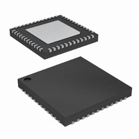
... Figure 10. CYWUSB6934/CYWUSB6932, 48 QFN – Top View RFOUT * E-PAD BOTTOM SIDE ** CYWUSB6934 Only Document 38-16007 Rev. *J CYWUSB6934/CYWUSB6932 Top View CYWUSB6934/CYWUSB6932 QFN CYWUSB6934 CYWUSB6932 X13IN 34 PACTL X13OUT 25 SCK Page [+] Feedback ...
Page 24
... Max. value measured with V = 3.3V CC Document 38-16007 Rev. *J +0.3V CC +0.3V CC Description Conditions –100.0 µ –2 2 < V < LOW PD = HIGH [12] no handshake [13] with handshaking CYWUSB6934 CYWUSB6932 [11] Min. Typ. Max. 2.7 3.0 3.6 – 0 2.4 3.0 0.0 0.4 [10] 2 –0.3 0.8 –1 0. 3.5 ...
Page 25
... SCK must start low, otherwise the success of SPI transactions are not guaranteed. Document 38-16007 Rev. *J Description Figure 11. SPI Timing Diagram fro SCK_LO SCK_H I (BURST READ) th every 9 SCK_HI data DAT_VAL CYWUSB6934 CYWUSB6932 Min. Typ. Max. Unit 476 ns 238 ns 158 ns 158 [17 [17] [17] 77 ...
Page 26
... Figure 13. DIO Receive Timing Diagram Figure 14. DIO Transmit Timing Diagram _IR _IR Q _LO data X_D X_D IO VA L_S CYWUSB6934 CYWUSB6932 Typ. Max. Unit µs µs 0 µs 0 µs 8 µs 16 µs 32 µs 8 µs 16 µs 32 µs Typ. Max. Unit 6.1 µ ...
Page 27
... C = –67 dBm C = –67 dBm [22 –67 dBm [22 –67 dBm Δ –64 dBm 5,10 MHz seven steps, monotonic PN Code Pattern 10101010 PN Code Pattern 11110000 100-kHz resolution bandwidth, –6 dBc CYWUSB6934 CYWUSB6932 Min. Typ. Max. Unit 2.400 2.483 GHz –3 ) –90 dBm –20 –10 dBm 28– ...
Page 28
... Figure 15. Power On Reset/Reset Timing Figure 16. Sleep / Wake Timing t WAKE t WAKE_INT Figure 16 illustrates a wakeup event configured to trigger an IRQ pin event via the Wake Enable register CYWUSB6934 CYWUSB6932 [28] Min. Typ Max. Unit 2000 µs 1 µs 1300 µs 1 µ ...
Page 29
... R2 937 R 500 3.00 CC Ordering Information Table 41. Ordering Information Part Number Radio CYWUSB6932-48LFXC Transmitter CYWUSB6934-48LFXC Transceiver CYWUSB6934-48LTXC Transceiver Document 38-16007 Rev Test Load OUTPUT 5 pF OUTPUT INCLUDING JIG AND Typical SCOPE Unit V CC 90% Ω 10% Ω GND Ω Rise time: 1 V/ns ...
Page 30
... Package Description Figure 18. 48-pin Lead-Free QFN LY48 (Punched) The recommended dimension of the PCB pad size for the E-PAD underneath the QFN is 209 mils × 209 mils (width x length). Document 38-16007 Rev. *J CYWUSB6934 CYWUSB6932 51-85152 *C Page [+] Feedback ...
Page 31
... Figure 19. 48-pin QFN 1.0 mm LT48C (Sawn) Document 38-16007 Rev. *J CYWUSB6934 CYWUSB6932 001-53698 ** Page [+] Feedback ...
Page 32
... Document History Page Document Title: CYWUSB6932/CYWUSB6934 WirelessUSB™ LS 2.4 GHz DSSS Radio SoC Document Number: 38-16007 Orig. of Submission Revision ECN Change ** 123907 LXA 01/20/03 *A 125470 XGR 04/28/03 *B 127076 KKU 07/30/03 *C 128886 KKV 08/04/03 *D 129180 TGE 12/04/03 *E 131851 TGE 12/15/03 *F 241471 ZTK ...
Page 33
... Cypress against all charges. Use may be limited by and subject to the applicable Cypress software license agreement. Document 38-16007 Rev. *J All products and company names mentioned in this document may be the trademarks of their respective holders. psoc.cypress.com clocks.cypress.com image.cypress.com Revised October 1, 2009 CYWUSB6934 CYWUSB6932 Page [+] Feedback ...