LMX9830SM/NOPB National Semiconductor, LMX9830SM/NOPB Datasheet
LMX9830SM/NOPB
Specifications of LMX9830SM/NOPB
*LMX9830SM/NOPB
LMX9830SM
Available stocks


Related parts for LMX9830SM/NOPB


LMX9830SM/NOPB Summary of contents
Page 1
... High integration: — Implemented in 0.18 μm CMOS technology — RF includes antenna filter and switch on-chip Bluetooth ® registered trademark of Bluetooth SIG, Inc. and is used under license by National Semiconductor Corporation. CompactRISC ® registered trademark of National Semiconductor Corporation. © 2008 National Semiconductor Corporation 3 ...
Page 2
Event filter 3.3 DIGITAL SMART RADIO ■ Accepts external clock or crystal input: — 13 MHz Typical — Supports MHz — Secondary 32.768 kHz oscillator for low-power modes — 20 ppm cumulative clock error required for ...
Page 3
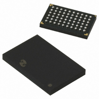
Connection Diagram FBGA, Plastic, Laminate, 9x6x1.2mm, 60 Ball, 0.8mm Pitch Package (SLF60A) 7.1 PAD DESCRIPTIONS Pad Name Pad Location X1_CKO F7 X1_CKI E7 X2_CKI F5 X2_CKO E5 RESET_RA# B8 B_RESET_RA# B6 RESET_BB# B7 ENV1 TST1/DIV2# B10 ...
Page 4
Pad Name Pad Location OP7/SDA/ D4 MDIDO OP3/MWCS# D3 OP4/PG4 D6 OP5 F4 SCLK F1 SFS F2 SRD F3 STD E3 XOSCEN A6 PG6 A7 PG7 D2 CTS#(Note 3) C2 RXD B3 RTS#(Note 4) B1 TXD C3 RDY# A4 TCK ...
Page 5
... The following conditions are true unless otherwise stated in the tables below: • -40°C to +85°C A • 3.3V CC • RF system performance specifications are guaranteed on National Semiconductor Mesa board rev 1.1 reference design platform. TABLE 2. Absolute Maximum Ratings Parameter TABLE 3. Recommended Operating Conditions Parameter grounded Min Max -0 ...
Page 6
... All tests are measured at antenna port unless otherwise specified • -40°C to +85°C A • VDD_RF = 2.8V unless otherwise specified. RF system performance specifications are guaranteed on National Semiconductor Mesa Board rev 1.1 reference design platform. Symbol Parameter RX Receive Sensitivity sense P RF Maximum Input Level ...
Page 7
Symbol Parameter Z (Note 15) Input Impedance of RF Port RFIN (RF_inout) Return Loss Return Loss (Note 15) OOB (Note 14), Out Of Band Blocking (Note 15) Performance Note 13: Typical operating conditions are at 2.75V operating voltage and 25°C ...
Page 8
Symbol f VCO Frequency Range VCO t Lock Time LOCK Δf Initial Carrier Frequency Tolerance offset (Note 21) 0 Δf Initial Carrier Frequency Drift drift (Note 21 Transmitter Delay Time D Note 21: Frequency accuracy is ...
Page 9
Front-End Bandpass Filter Response TX and RX Pin 50Ω Impedance Characteristics 9 20180050 20180007 www.national.com ...
Page 10
Functional Description 9.1 BASEBAND AND LINK MANAGEMENT PROCESSORS Baseband and Lower Link control functions are implemented using a combination of National’s CompactRISC 16-bit pro- cessor and the Bluetooth Lower Link Controller. These pro- cessors operate from integrated ROM memory ...
Page 11
External memory interfaces As the LMX9830 is a ROM based device with no on-chip non volatile storage, the operation parameters will be lost after a power cycle or hardware reset. In order to prevent re initial- izing such parameters, ...
Page 12
Item Range Baud Rate 2.4 to 921.6 kbits/s Flow Control RTS#/CTS# or None Parity Odd, Even, None Stop Bits 1,2 Data Bits 8 9.3 AUDIO PORT 9.3.1 Advanced Audio Interface The Advanced Audio Interface (AAI advanced version of ...
Page 13
In alternate function the pins have pre-defined indication func- tionality. Please see Table 13 for a description on the alter- nate indication functionality. Pin OP4/PG4 Operation Mode pin to configure Transport Layer settings during boot-up PG6 GPIO PG7 RF Traffic ...
Page 14
ESR (Ω Note 30: Frequency, loading caps and ESR all must be considered for determining startup time. Note 31: For reference only, must be tested on each system to accurately design POR and correctly startup ...
Page 15
FIGURE 2. Flow Diagram for the Start-up Sequence 15 20180010 www.national.com ...
Page 16
Osc Freq. (MHz) BBCLK (MHz 10-20 (Note 38) 10-20 (Note 35 Note 35: If OP3 is 1, must use 1k Ω pull up. Note 36: If OP4 is 1, must ...
Page 17
USING AN EXTERNAL EEPROM FOR NON-VOLATILE DATA The LMX9830 offers two interfaces to connect to external memory. Depending on the EEPROM used, the interface is activated by setting the correct option pins during start up. See Table 16 for ...
Page 18
Digital Smart Radio 10.1 FUNCTIONAL DESCRIPTION The integrated Digital Smart Radio utilizes a heterodyne re- ceiver architecture with a low intermediate frequency (2 MHz) such that the intermediate frequency filters can be integrated on chip. The receiver consists of ...
Page 19
IQ-DA Converters and TX Mixers The ROM output signals drive an I- and a Q-DA converter. Two Butterworth low-pass filters filter the DA output signals. The 6 MHz clock for the DA converters and the logic circuitry around the ...
Page 20
FIGURE 5. Crystal Equivalent Circuit Specification Package Frequency Mode Stability C Load Capacitance L ESR C Shunt Capacitance 0 Drive Level Pullability Storage Temperature Reference Ct1 Ct2 FIGURE 6. Frequency Offset with 12 pF//12 pF Capacitors www.national.com 20180013 TABLE 18. ...
Page 21
FIGURE 7. Frequency Offset with 10 pF//10 pF Capacitors 10.7.2 TCXO (Temperature Compensated Crystal Oscillator) The LMX9830 also can operate with an external TCXO (Tem- perature Compensated Crystal Oscillator). The TCXO signal is directly connected to the CLK+. 1. Input ...
Page 22
ESR (Equivalent Series Resistance) LMX9830 can operate with a wide range of crystals with dif- ferent ESR ratings. Reference Table 21 and Figure 9 for more details. Parameter External Reference Clock Frequency (Note 39) Frequency Tolerance (over full operating ...
Page 23
LOOP FILTER DESIGN The LMX9830 has an external loop filter which must be de- signed for best performance by the end customer. This sec- 10.9.1 Component Calculations The following parameters are required for component value calculation of a third ...
Page 24
Summary: Symbol n N counter value Loop Bandwidth T1 Loop filter pole T2 Loop filter zero T3 Loop filter zero A0 Total capacitance A1 First order loop filter coefficient A2 Second order loop filter coefficient Components can then be calculated ...
Page 25
Even further out from the carrier, the phase noise will be mainly dominated by the VCO noise assuming the crystal is relatively clean. These equations are ...
Page 26
Original results: Hoppong On- Low Channel Drift Rate/50 μs15.00 15.00 kHz Maximum Drift 19 kHz Average Drift 11 kHz Packets Tested 10 Packets Failed 0 Result Pass Hoppong On- Med Channel Drift Rate/50 μs 15.00 kHz Max Drift 19 kHz ...
Page 27
New results: Hoppong On- Low Channel DH1 Drift Rate/50 μs −12.00 kHz Max Drift −15 kHz Average Drift −6 kHz Packets Tested 10 Packets Failed 0 Overall Result Pass Hoppong On- Med Channel DH1 Drift Rate/50 μs −14.20 kHz Max ...
Page 28
Integrated Firmware The LMX9830 includes the full Bluetooth stack up to RF- Comm to support the following profiles: • GAP (Generic Access Profile) • SDAP (Service Discovery Application Profile) • SPP (Serial Port Profile) Figure 12 shows the Bluetooth ...
Page 29
TABLE 22. Operation Parameters Stored in LMX9830 Parameter Default Value BDADDR (To be requested from IEEE) Local Name Serial port device PinCode 0000 Operation Mode Automatic ON Default Connections 0 SDP Database 1 SPP entry: Name: COM1 Authentication and encryption ...
Page 30
Low Power Modes The LMX9830 supports different Low Power Modes to reduce power in different operating situations. The modular structure of the LMX9830 allows the firmware to power down unused modules. The Low power modes have influence on: • ...
Page 31
ENABLING AND DISABLING UART TRANSPORT 12.2.1 Hardware Wake up functionality In certain usage scenarios the host is able to switch off the transport layer of the LMX9830 in order to reduce power con- sumption. Afterwards both devices, host and ...
Page 32
StartD Packet elimiter Type ID 1 Byte 1 Byte - - - - - - - - - - - - - Checksum - - - - - - - - - - - - - ID Direction 0x52 REQUEST ...
Page 33
Command Connect Default Connection Connect Default Connection Confirm Connects to either one or all stored default connections Store Default Connection Store Default Connection Confirm Get list of Default Connections List of Default Devices Delete Default Connections Delete Default Connections Confirm ...
Page 34
Command Set Port Config Set Port Config Confirm Get Port Config Get Port Config Confirm Port Config Changed SPP Get Port Status SPP Get Port Status Confirm SPP Port Set DTR SPP Port Set DTR Confirm SPP Port Set RTS ...
Page 35
Command Get Default Audio Settings Get Default Audio Settings Confirm Set Default Audio Settings Set Default Audio Settings Confirm Set Event Filter Set Event Filter Confirm Get Event Filter Get Event Filter Confirm Read RSSI Read RSSI Confirm Change UART ...
Page 36
Usage Scenarios 14.1 SCENARIO 1: POINT-TO-POINT CONNECTION LMX9830 acts only as slave, no further configuration is re- quired. Example: Sensor with LMX9830; hand-held device with stan- dard Bluetooth option. www.national.com The SPP conformance of the LMX9830 allows any device ...
Page 37
SCENARIO 2: AUTOMATIC POINT-TO-POINT CONNECTION LMX9830 at both sides. Example: Serial Cable Replacement. Device #1 controls the link setup with a few commands as described. If step 5 is executed, the stored default device is connected (step 4) after ...
Page 38
SCENARIO 3: POINT-TO-MULTIPOINT CONNECTION LMX9830 acts as master for several slaves. Example: Two sensors with LMX9830; one hand-held device with implemented LMX9830. Serial Devices #2 and #3 establish the link automatically as soon as they are contacted by another ...
Page 39
Application Information Figure 19 represents a typical system functional schematic for the LMX9830 in its normal 3.0V or 3.3V system interface operation. In Figure 20 represents a typical system functional schematic for the LMX9830 in its 1.8V system interface ...
Page 40
Note 40: Capacitor values, Ct1 and Ct2 may vary depending on board design crystal manufacturer specification. Note crystal capacitance load rating) of 12pF or greater rating is required from the crystal vendor of choice to best match module ...
Page 41
Note 41: Capacitor values, Ct1 and Ct2 may vary depending on board design crystal manufacturer specification. Note crystal capacitance load rating) of 12pF or greater rating is required from the crystal vendor of choice to best match module ...
Page 42
Reference Design Note: For a schematic including an RS232 communication with the host, please refer to the “LMX9830DONGLE designer guide”. Recommended that a 4 component T-PI pad be used be- tween RF out and antenna input. Allows for versatility ...
Page 43
Soldering The LMX9830 bumps are designed to melt as part of the Sur- face Mount Assembly (SMA) process. In order to ensure reflow of all solder bumps and maximum solder joint reliability while minimizing damage to the package, recommended ...
Page 44
www.national.com 44 ...
Page 45
Physical Dimensions FBGA, Plastic, Laminate, 9x6x1.2mm, 60 Ball, 0.8mm Pitch Package inches (millimeters) unless otherwise noted NS Package Number SLF60A 45 www.national.com ...
Page 46
... For more National Semiconductor product information and proven design tools, visit the following Web sites at: Products Amplifiers www.national.com/amplifiers Audio www.national.com/audio Clock Conditioners www.national.com/timing Data Converters www.national.com/adc Displays www.national.com/displays Ethernet www.national.com/ethernet Interface www.national.com/interface LVDS www.national.com/lvds Power Management www.national.com/power Switching Regulators www.national.com/switchers LDOs www ...