LMX9830SM/NOPB National Semiconductor, LMX9830SM/NOPB Datasheet - Page 3
LMX9830SM/NOPB
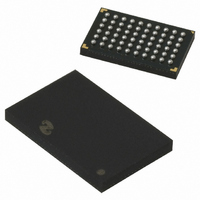
Manufacturer Part Number
LMX9830SM/NOPB
Description
IC SRL PORT MOD BLUETOOTH 60FBGA
Manufacturer
National Semiconductor
Datasheet
1.LMX9830SMNOPB.pdf
(46 pages)
Specifications of LMX9830SM/NOPB
Frequency
2.4GHz
Data Rate - Maximum
704kbps
Modulation Or Protocol
Bluetooth v2.0, Class 2
Applications
PDA's, POS Terminals
Power - Output
0dBm
Sensitivity
-80dBm
Voltage - Supply
2.5 V ~ 3.6 V
Current - Receiving
65mA
Current - Transmitting
65mA
Data Interface
PCB, Surface Mount
Antenna Connector
PCB, Surface Mount
Operating Temperature
-40°C ~ 125°C
Package / Case
60-FBGA
Physical Interfaces
UART
Data Rate
704Kbps
Operating Temperature Range
-40°C To +125°C
Msl
MSL 4 - 72 Hours
Supply Voltage Range
1.6V To 3.6V
Frequency Max
2480MHz
Termination Type
SMD
Rohs Compliant
Yes
Filter Terminals
SMD
Frequency Min
2402MHz
Lead Free Status / RoHS Status
Lead free / RoHS Compliant
Memory Size
-
Lead Free Status / Rohs Status
Compliant
Other names
*LMX9830SM
*LMX9830SM/NOPB
LMX9830SM
*LMX9830SM/NOPB
LMX9830SM


X1_CKO
X1_CKI
X2_CKI
X2_CKO
RESET_RA#
B_RESET_RA#
RESET_BB#
ENV1#
TE
TST1/DIV2#
TST2
TST3
TST4
TST5
TST6
MDODI (Note 2)
OP6/SCL/MSK
7.0 Connection Diagram
7.1 PAD DESCRIPTIONS
Pad Name
Pad Location
FBGA, Plastic, Laminate, 9x6x1.2mm, 60 Ball, 0.8mm Pitch Package (SLF60A)
B10
E7
E5
B8
B6
B7
C6
A9
C7
C8
C9
D8
D9
D1
C1
F7
F5
SCL/MSK: I/O
OP6: I
Type
I/O
O
O
O
I
I
I
I
I
I
I
I
I
I
I
I
TABLE 1. Pin Descriptions
Default Layout
See Table 16
(if not used)
(if not used)
VCO_OUT
GND
GND
GND
GND
GND
GND
NC
NC
NC
NC
3
Crystal 10-20 MHz
Crystal or External Clock 10-20 MHz
32.768 kHz Crystal Oscillator
32.768 kHz Crystal Oscillator
Radio Reset (active low)
Buffered Reset Radio Output (active low)
Baseband Reset (active low)
ENV1: Environment Select (active low) used for
manufacturing test only
Test Enable - Used for manufacturing test only
TST1: Test Mode. Leave not connected to permit use
with VTune automatic tuning algorithm
DIV2#: No longer supported
Test Mode, Connect to GND
Test Mode, Connect to GND
Test Mode, Connect to GND
Test Mode, Connect to GND
Test Input,
Connect to VCO_OUT via 0 Ω resistor to permit use
with VTune automatic tuning algorithm
SPI Master Out Slave In
OP6: Pin checked during Startup Sequence for
configuration option
SCL: ACCESS.Bus Clock
MSK: SPI Shift
Description
www.national.com
20180001
Related parts for LMX9830SM/NOPB
Image
Part Number
Description
Manufacturer
Datasheet
Request
R

Part Number:
Description:
Manufacturer:
National Semiconductor
Datasheet:

Part Number:
Description:
National Semiconductor [8-Bit D/A Converter]
Manufacturer:
National Semiconductor
Datasheet:
Part Number:
Description:
National Semiconductor [Media Coprocessor]
Manufacturer:
National Semiconductor
Datasheet:
Part Number:
Description:
Digitally Controlled Tone and Volume Circuit with Stereo Audio Power Amplifier, Microphone Preamp Stage and National 3D Sound
Manufacturer:
National Semiconductor
Datasheet:
Part Number:
Description:
Digitally Controlled Tone and Volume Circuit with Stereo Audio Power Amplifier, Microphone Preamp Stage and National 3D Sound
Manufacturer:
National Semiconductor
Datasheet:
Part Number:
Description:
AC97 Rev 2 Codec with Sample Rate Conversion and National 3D Sound
Manufacturer:
National Semiconductor
Part Number:
Description:
Manufacturer:
National Semiconductor
Datasheet:
Part Number:
Description:
Manufacturer:
National Semiconductor
Datasheet:
Part Number:
Description:
General Purpose, Low Voltage, Low Power, Rail-to-Rail Output Operational Amplifiers
Manufacturer:
National Semiconductor
Datasheet:
Part Number:
Description:
8-bit 20 MSPS flash A/D converter.
Manufacturer:
National Semiconductor
Datasheet:
Part Number:
Description:
Low Noise Quad Operational Amplifier
Manufacturer:
National Semiconductor
Datasheet:
Part Number:
Description:
Quad Differential Line Receivers
Manufacturer:
National Semiconductor
Datasheet:
Part Number:
Description:
Quad High Speed Trapezoidal? Bus Transceiver
Manufacturer:
National Semiconductor
Datasheet:
Part Number:
Description:
Dual Line Receiver
Manufacturer:
National Semiconductor
Datasheet: