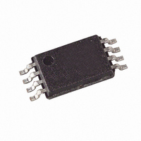
T48C862M-R4-TNQ Atmel, T48C862M-R4-TNQ Datasheet - Page 30

T48C862M-R4-TNQ
Manufacturer Part Number
T48C862M-R4-TNQ
Description
IC MON TIRE PRESS 433MHZ 24-SOIC
Manufacturer
Atmel
Datasheet
1.T48C862M-R4-TNS.pdf
(107 pages)
Specifications of T48C862M-R4-TNQ
Frequency
433MHz
Modulation Or Protocol
FM, FSK
Data Rate - Maximum
32 kBaud
Power - Output
10dBm
Current - Transmitting
9.5mA
Data Interface
PCB, Surface Mount
Antenna Connector
PCB, Surface Mount
Memory Size
1KB EEPROM, 1KB RAM
Voltage - Supply
2 V ~ 4 V
Operating Temperature
-40°C ~ 125°C
Package / Case
24-SOIC (0.200", 5.30mm Width)
Lead Free Status / RoHS Status
Contains lead / RoHS non-compliant
Features
-
Applications
-
Peripheral Modules
Addressing Peripherals
30
T48C862-R4 [Preliminary]
The microcontroller block has various power-down modes. During the sleep mode the
clock for the microcontroller block core is stopped. With the NSTOP bit in the clock man-
agement register (CM), it is programmable if the clock for the on-chip peripherals is
active or stopped during the sleep mode. If the clock for the core and the peripherals is
stopped, the selected oscillator is switched off. An exception is the 32-kHz oscillator, if it
is selected it runs continuously independent of the NSTOP bit. If the oscillator is stopped
or the 32-kHz oscillator is selected, power consumption is extremely low.
Table 8. Power-down Modes
Accessing the peripheral modules takes place via the I/O bus (see Figure 27 on page
31). The IN or OUT instructions allow direct addressing of up to 16 I/O modules. A dual
register addressing scheme has been adopted to enable direct addressing of the pri-
mary register. To address the auxiliary register, the access must be switched with an
auxiliary switching module. Thus, a single IN (or OUT) to the module address will read
(or write into) the module primary register. Accessing the auxiliary register is performed
with the same instruction preceded by writing the module address into the auxiliary
switching module. Byte wide registers are accessed by multiple IN- (or OUT-) instruc-
tions. For more complex peripheral modules, with a larger number of registers,
extended addressing is used. In this case, a bank of up to 16 subport registers are indi-
rectly addressed with the subport address. The first OUT instruction writes the subport
address to the sub address register, the second IN or OUT instruction reads data from
or writes data to the addressed subport.
Note:
SLEEP
Power-
Active
Mode
down
1. Osc-Stop = SLEEP and NSTOP and WDL
SLEEP
SLEEP
Core
CPU
RUN
Stop
Osc-
YES
NO
NO
(1)
Function
Brown-
Active
Active
STOP
out
RC-oscillator 1
RC-oscillator 2
Oscillator
4-MHz
STOP
RUN
RUN
Oscillator
32-kHz
RUN
RUN
RUN
4551C–4BMCU–01/04
External
Clock
STOP
Input
YES
YES


