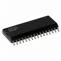
CLRC63201T/0FE,112 NXP Semiconductors, CLRC63201T/0FE,112 Datasheet - Page 8

CLRC63201T/0FE,112
Manufacturer Part Number
CLRC63201T/0FE,112
Description
IC I.CODE HS READER 32-SOIC
Manufacturer
NXP Semiconductors
Series
I-Coder
Specifications of CLRC63201T/0FE,112
Rf Type
Read Only
Frequency
13.56MHz
Features
ISO14443-A, ISO14443-B, ISO15693, ISO18000-3
Package / Case
32-SOIC (0.300", 7.50mm Width)
Product
RFID Readers
Operating Temperature Range
- 25 C to + 85 C
Lead Free Status / RoHS Status
Lead free / RoHS Compliant
Lead Free Status / RoHS Status
Lead free / RoHS Compliant, Lead free / RoHS Compliant
Other names
568-2199-5
935269690112
CLRC632
CLRC63201TD
935269690112
CLRC632
CLRC63201TD
Available stocks
Company
Part Number
Manufacturer
Quantity
Price
Company:
Part Number:
CLRC63201T/0FE,112
Manufacturer:
IR
Quantity:
3 400
Part Number:
CLRC63201T/0FE,112
Manufacturer:
NXP/恩智浦
Quantity:
20 000
Philips Semiconductors
Multiple Protocol Contactless Reader IC
3.2.5 RESET PIN
The reset pin disables internal current sources and clocks and detaches the CL RC632 virtually from the µC
bus. If RST is released, the CL RC632 executes the power up sequence.
3.2.6 OSCILLATOR
Name
XIN
XOUT
The very fast on-chip oscillator buffer operates with a 13.56 MHz crystal connected to XIN and XOUT. If the
device shall operate with an external clock it may be applied to pin XIN.
3.2.7 MIFARE INTERFACE
The CL RC632 supports the active antenna concept of MIFARE
NPAUSE and KOMP of MIFARE
Name
MFIN
MFOUT
The MIFARE
RC632 separately in the following ways:
Note: The SL RC400 uses the name SIGOUT for the MFOUT pin. The CLRC 632 functionality includes the
test possibilities for the SL RC 400 using the pin MFOUT.
3.2.8 PARALLEL INTERFACE
16 pins control the parallel interface:
Name
D0
A0 … A2
NWR / RNW
NRD / NDS
NCS
ALE
The analog circuit may be used stand-alone via the MIFARE
connected to the externally generated NPAUSE signal. The MFOUT pin provides the KOMP signal.
The digital circuit may be used to drive an external analog circuit via the MIFARE
the MFOUT pin provides the internally generated NPAUSE signal and MFIN will be connected to the
KOMP signal from the outside.
D7
®
interface may be used to communicate with either the analog or the digital part of the CL
®
Core Modules (MF CMxxx) at the pins MFIN and MFOUT.
Type
I
O
Type
I with Schmitt Trigger
O
Type
I/O with Schmitt Trigger
I/O with Schmitt Trigger
I/O with Schmitt Trigger
I/O with Schmitt Trigger
I/O with Schmitt Trigger
I/O with Schmitt Trigger
8
®
®
Short Form Specification Rev. 3.2 April 2005
. It may handle the base-band signals
interface. In that case MFIN will be
Function
Oscillator Buffer Input
Oscillator Buffer Output
Function
MIFARE
MIFARE
Signal Output
Function
Bi-directional Data Bus
Address Lines
Not Write / Read Not Write
Not Read / Not Data Strobe
Not Chip Select
Address Latch Enable
®
®
Interface Input
Interface Output
®
interface. In that case
CL RC632
PUBLIC


