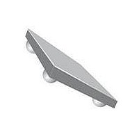
USBULC6-3F3 STMicroelectronics, USBULC6-3F3 Datasheet

USBULC6-3F3
Specifications of USBULC6-3F3
Available stocks
Related parts for USBULC6-3F3
USBULC6-3F3 Summary of contents
Page 1
... High speed USB port in wireless handsets (up to 480 Mb/s according to USB 2.0 high speed specification) Description The USBULC6-3F3 is a monolithic, application specific discrete device dedicated to ESD protection of high speed interfaces. Its ultralow line capacitance secures a high level of signal integrity without compromising the protection of downstream sensitive chips against the most stringently characterized ESD strikes ...
Page 2
... I/O to GND ID (B2 bump OSC 2/10 amb Parameter Parameter Breakdown voltage Leakage current @ V RM Stand-off voltage I/O to GND capacitance = 25 °C) amb Test conditions = OSC = MHz RMS Doc ID 17596 Rev 1 USBULC6-3F3 = 25 °C) Value 8 T initial = amb 2.5 125 - -55 to +150 ...
Page 3
... USBULC6-3F3 Figure 3. Relative variation of peak pulse power versus initial junction temperature (typical value 100 Figure 5. Clamping voltage versus peak pulse current (typical values, exponential waveform) I (A) PP 10.0 T initial = 25 °C j 8/20 µs 1.0 0 Figure 7. Junction capacitance versus reverse voltage applied (typical values) C(pF) 2 ...
Page 4
... Figure 10. S21 (dB) attenuation (° 100 125 300k 1M Figure 12. ESD response to IEC 61000-4-2 (-8 kV contact discharge V/div 20 ns/div Figure 14. Eye diagram PCB + USBULC6-3F3 400 mV amplitude 480 Mbps 100 m/div 348 ps/div Doc ID 17596 Rev 1 USBULC6-3F3 F(Hz) 3M 10M 30M 100M 300M ns/div 348 ps/div ...
Page 5
... USBULC6-3F3 2 Application schematic example Figure 15. Schematic example V BUS GND Application schematic example Data Data ID GND Doc ID 17596 Rev 1 5/10 ...
Page 6
... Ordering information scheme 3 Ordering information scheme Figure 16. Ordering information scheme 3 = Lead-free, pitch = 400 µm, bump = 255 µm 6/10 USB USB protection Ultra low capacitance Breakdown voltage min Number of lines lines Package F = Flip Chip Doc ID 17596 Rev 1 USBULC6-3F3 ULC ...
Page 7
... USBULC6-3F3 4 Package information In order to meet environmental requirements, ST offers these devices in different grades of ® ECOPACK packages, depending on their level of environmental compliance. ECOPACK specifications, grade definitions and product status are available at: www.st.com. ® ECOPACK trademark. Figure 17. Package dimensions 210 µm Figure 18. Footprint recommendations Copper pad Diameter: 220 µ ...
Page 8
... Tape and reel specification 5 Tape and reel specification Figure 20. Flip Chip tape and reel specifications Dot identifying Pin A1 location 0.20 0.69 All dimensions are typical values in mm 8/10 2.0 4.0 0.92 2.0 User direction of unreeling Doc ID 17596 Rev 1 USBULC6-3F3 Ø 1.55 ...
Page 9
... USBULC6-3F3 6 Ordering information Table 3. Ordering information Order code USBULC6-3F3 7 Revision history Table 4. Document revision history Date 01-Jul-2010 Marking Package EV Flip Chip 0.86 mg Revision 1 Initial release. Doc ID 17596 Rev 1 Ordering information Weight Base qty Delivery mode 5000 Tape and reel Changes 9/10 ...
Page 10
... Australia - Belgium - Brazil - Canada - China - Czech Republic - Finland - France - Germany - Hong Kong - India - Israel - Italy - Japan - Malaysia - Malta - Morocco - Philippines - Singapore - Spain - Sweden - Switzerland - United Kingdom - United States of America 10/10 Please Read Carefully: © 2010 STMicroelectronics - All rights reserved STMicroelectronics group of companies www.st.com Doc ID 17596 Rev 1 USBULC6-3F3 ...


