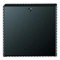
PIC18F6585-I/L Microchip Technology, PIC18F6585-I/L Datasheet - Page 140

PIC18F6585-I/L
Manufacturer Part Number
PIC18F6585-I/L
Description
Microcontrollers (MCU) 48KB 3328 RAM 52 I/O
Manufacturer
Microchip Technology
Datasheet
1.PCM18XK1.pdf
(496 pages)
Specifications of PIC18F6585-I/L
Processor Series
PIC18F
Core
PIC
Data Bus Width
8 bit
Data Ram Size
3.25 KB
Interface Type
I2C/SPI/AUSART/CAN
Maximum Clock Frequency
40 MHz
Number Of Programmable I/os
53
Number Of Timers
5
Maximum Operating Temperature
+ 85 C
Mounting Style
SMD/SMT
3rd Party Development Tools
52715-96, 52716-328, 52717-734, 52712-325, EWPIC18
Development Tools By Supplier
PG164130, DV164035, DV244005, DV164005, PG164120, ICE2000, ICE4000, DV164136, DM183032
Minimum Operating Temperature
- 40 C
On-chip Adc
12-ch x 10-bit
Program Memory Type
Flash
Program Memory Size
48 KB
Package / Case
PLCC-68
Lead Free Status / RoHS Status
Lead free / RoHS Compliant
- Current page: 140 of 496
- Download datasheet (9Mb)
PIC18F6585/8585/6680/8680
TABLE 10-9:
TABLE 10-10: SUMMARY OF REGISTERS ASSOCIATED WITH PORTE
DS30491C-page 138
RE0/RD/AD8
RE1/WR/AD9
RE2/CS/AD10
RE3/AD11
RE4/AD12
RE5/AD13/
RE6/AD14/
RE7/CCP2/AD15
Legend: ST = Schmitt Trigger input, TTL = TTL input
Note 1:
TRISE
PORTE
LATE
MEMCON
PSPCON
Legend: x = unknown, u = unchanged. Shaded cells are not used by PORTE.
Name
2:
3:
Name
(2)
(2)
Input buffers are Schmitt Triggers when in I/O or CCP mode, and TTL buffers when in System Bus or PSP
Control mode.
Available in PIC18F8X8X devices only.
On PIC18F8X8X devices, these pins may be moved to RHY or RH6 by changing the ECCPMX
configuration bit.
(2)
(2)
PORTE Data Direction Control Register
Read PORTE Data Latch/Write PORTE Data Latch
Read PORTE pin/Write PORTE Data Latch
(2)
EBDIS
P1C
P1B
(2)
Bit 7
(2)
IBF
(2)
(3)
(3)
PORTE FUNCTIONS
Bit#
bit 0
bit 1
bit 2
bit 3
bit 4
bit 5
bit 6
bit 7
Bit 6
OBF
—
Buffer Type
WAIT1
IBOV
Bit 5
ST/TTL
ST/TTL
ST/TTL
ST/TTL
ST/TTL
ST/TTL
ST/TTL
ST/TTL
(1)
(1)
(1)
(1)
(1)
(1)
(1)
(1)
PSPMODE
WAIT0
Bit 4
Input/output port pin, read control for Parallel Slave Port or
address/data bit 8.
For RD (PSP Control mode):
1 = Not a read operation
0 = Read operation, reads PORTD register (if chip selected)
Input/output port pin, write control for Parallel Slave Port or
address/data bit 9.
For WR (PSP Control mode):
1 = Not a write operation
0 = Write operation, writes PORTD register (if chip selected)
Input/output port pin, chip select control for Parallel Slave Port or
address/data bit 10.
For CS (PSP Control mode):
1 = Device is not selected
0 = Device is selected
Input/output port pin or address/data bit 11.
Input/output port pin or address/data bit 12.
Input/output port pin, address/data bit 13 or ECCP1 PWM output C.
Input/output port pin, address/data bit 13 or ECCP1 PWM output B.
Input/output port pin, Capture 2 input/Compare 2 output/PWM output
(PIC18F8X20 devices in Microcontroller mode only) or
address/data bit 15.
Bit 3
—
—
Bit 2
—
—
WM1
Bit 1
—
Function
WM0
Bit 0
—
2004 Microchip Technology Inc.
POR, BOR
1111 1111
xxxx xxxx
xxxx xxxx
0-00 --00
0000 ----
Value on:
1111 1111
uuuu uuuu
uuuu uuuu
0000 --00
0000 ----
Value on
all other
Resets
Related parts for PIC18F6585-I/L
Image
Part Number
Description
Manufacturer
Datasheet
Request
R

Part Number:
Description:
20-Pin USB Flash Microcontrollers
Manufacturer:
MICROCHIP [Microchip Technology]
Datasheet:

Part Number:
Description:
PIC18F With 128-segment LCD Driver And 12-bit ADC, 8KB Flash, 768B RAM, CCP, MSS
Manufacturer:
Microchip Technology
Datasheet:

Part Number:
Description:
PIC18F With 128-segment LCD Driver And 12-bit ADC, 16KB Flash, 768B RAM, CCP, MS
Manufacturer:
Microchip Technology
Datasheet:

Part Number:
Description:
PIC18F With 192-segment LCD Driver And 12-bit ADC, 8KB Flash, 768B RAM, CCP, MSS
Manufacturer:
Microchip Technology
Datasheet:

Part Number:
Description:
PIC18F With 192-segment LCD Driver And 12-bit ADC, 16KB Flash, 768B RAM, CCP, MS
Manufacturer:
Microchip Technology
Datasheet:

Part Number:
Description:
Microcontrollers (MCU) 64KB 3328 RAM 52 I/O
Manufacturer:
Microchip Technology
Datasheet:

Part Number:
Description:
32kB Flash, 2kB RAM, 1kB EE, NanoWatt XLP, LCD 64 QFN 9x9x0.9mm T/R
Manufacturer:
Microchip Technology
Datasheet:

Part Number:
Description:
32kB Flash, 2kB RAM, 1kB EE, NanoWatt XLP, LCD 64 TQFP 10x10x1mm T/R
Manufacturer:
Microchip Technology
Datasheet:

Part Number:
Description:
128kB Flash, 4kB RAM, 1kB EE, 16MIPS, NanoWatt XLP, LCD, 5V 80 TQFP 12x12x1mm T/
Manufacturer:
Microchip Technology
Datasheet:

Part Number:
Description:
32kB Flash, 2kB RAM, 1kB EE, NanoWatt XLP, LCD 64 QFN 9x9x0.9mm TUBE
Manufacturer:
Microchip Technology
Datasheet:

Part Number:
Description:
32kB Flash, 2kB RAM, 1kB EE, NanoWatt XLP, LCD 64 TQFP 10x10x1mm TRAY
Manufacturer:
Microchip Technology

Part Number:
Description:
128kB Flash, 4kB RAM, 1kB EE, 16MIPS, NanoWatt XLP, LCD, 5V 80 TQFP 12x12x1mm TR
Manufacturer:
Microchip Technology

Part Number:
Description:
Manufacturer:
Microchip Technology Inc.
Datasheet:


