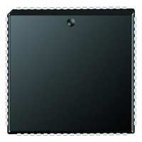
PIC18F6585-I/L Microchip Technology, PIC18F6585-I/L Datasheet - Page 183

PIC18F6585-I/L
Manufacturer Part Number
PIC18F6585-I/L
Description
Microcontrollers (MCU) 48KB 3328 RAM 52 I/O
Manufacturer
Microchip Technology
Datasheet
1.PCM18XK1.pdf
(496 pages)
Specifications of PIC18F6585-I/L
Processor Series
PIC18F
Core
PIC
Data Bus Width
8 bit
Data Ram Size
3.25 KB
Interface Type
I2C/SPI/AUSART/CAN
Maximum Clock Frequency
40 MHz
Number Of Programmable I/os
53
Number Of Timers
5
Maximum Operating Temperature
+ 85 C
Mounting Style
SMD/SMT
3rd Party Development Tools
52715-96, 52716-328, 52717-734, 52712-325, EWPIC18
Development Tools By Supplier
PG164130, DV164035, DV244005, DV164005, PG164120, ICE2000, ICE4000, DV164136, DM183032
Minimum Operating Temperature
- 40 C
On-chip Adc
12-ch x 10-bit
Program Memory Type
Flash
Program Memory Size
48 KB
Package / Case
PLCC-68
Lead Free Status / RoHS Status
Lead free / RoHS Compliant
- Current page: 183 of 496
- Download datasheet (9Mb)
16.2.5
In Full-Bridge Output mode, four pins are used as
outputs; however, only two outputs are active at a time.
In the Forward mode, pin P1A is continuously active
and pin P1D is modulated. In the Reverse mode, pin
PGC is continuously active and pin P1B is modulated.
These are illustrated in Figure 16-7.
FIGURE 16-7:
2004 Microchip Technology Inc.
Forward Mode
Reverse Mode
Note 1: At this time, the TMR2 register is equal to the PR2 register.
Note
FULL-BRIDGE MODE
2: Output signal is shown as active-high.
P1A
P1B
P1C
P1D
P1A
P1B
P1C
P1D
(2)
(2)
(2)
(2)
(2)
(2)
(2)
(2)
FULL-BRIDGE PWM OUTPUT
(1)
(1)
Duty Cycle
Duty Cycle
PIC18F6585/8585/6680/8680
Period
Period
P1A, P1B, P1C and P1D outputs are multiplexed with
the PORTC<2>, PORTE<6:5> and PORTG<4> data
latches. The TRISC<2>, TRISC<6:5> and TRISG<4>
bits must be cleared to make the P1A, P1B, P1C and
P1D pins outputs.
(1)
(1)
DS30491C-page 181
Related parts for PIC18F6585-I/L
Image
Part Number
Description
Manufacturer
Datasheet
Request
R

Part Number:
Description:
20-Pin USB Flash Microcontrollers
Manufacturer:
MICROCHIP [Microchip Technology]
Datasheet:

Part Number:
Description:
PIC18F With 128-segment LCD Driver And 12-bit ADC, 8KB Flash, 768B RAM, CCP, MSS
Manufacturer:
Microchip Technology
Datasheet:

Part Number:
Description:
PIC18F With 128-segment LCD Driver And 12-bit ADC, 16KB Flash, 768B RAM, CCP, MS
Manufacturer:
Microchip Technology
Datasheet:

Part Number:
Description:
PIC18F With 192-segment LCD Driver And 12-bit ADC, 8KB Flash, 768B RAM, CCP, MSS
Manufacturer:
Microchip Technology
Datasheet:

Part Number:
Description:
PIC18F With 192-segment LCD Driver And 12-bit ADC, 16KB Flash, 768B RAM, CCP, MS
Manufacturer:
Microchip Technology
Datasheet:

Part Number:
Description:
Microcontrollers (MCU) 64KB 3328 RAM 52 I/O
Manufacturer:
Microchip Technology
Datasheet:

Part Number:
Description:
32kB Flash, 2kB RAM, 1kB EE, NanoWatt XLP, LCD 64 QFN 9x9x0.9mm T/R
Manufacturer:
Microchip Technology
Datasheet:

Part Number:
Description:
32kB Flash, 2kB RAM, 1kB EE, NanoWatt XLP, LCD 64 TQFP 10x10x1mm T/R
Manufacturer:
Microchip Technology
Datasheet:

Part Number:
Description:
128kB Flash, 4kB RAM, 1kB EE, 16MIPS, NanoWatt XLP, LCD, 5V 80 TQFP 12x12x1mm T/
Manufacturer:
Microchip Technology
Datasheet:

Part Number:
Description:
32kB Flash, 2kB RAM, 1kB EE, NanoWatt XLP, LCD 64 QFN 9x9x0.9mm TUBE
Manufacturer:
Microchip Technology
Datasheet:

Part Number:
Description:
32kB Flash, 2kB RAM, 1kB EE, NanoWatt XLP, LCD 64 TQFP 10x10x1mm TRAY
Manufacturer:
Microchip Technology

Part Number:
Description:
128kB Flash, 4kB RAM, 1kB EE, 16MIPS, NanoWatt XLP, LCD, 5V 80 TQFP 12x12x1mm TR
Manufacturer:
Microchip Technology

Part Number:
Description:
Manufacturer:
Microchip Technology Inc.
Datasheet:


