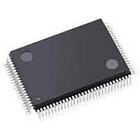
LCMXO640C-3TN100C Lattice, LCMXO640C-3TN100C Datasheet - Page 14

LCMXO640C-3TN100C
Manufacturer Part Number
LCMXO640C-3TN100C
Description
CPLD - Complex Programmable Logic Devices 640 LUTS 74 I/O
Manufacturer
Lattice
Series
MachXOr
Datasheet
1.LCMXO640C-3TN100C.pdf
(95 pages)
Specifications of LCMXO640C-3TN100C
Memory Type
SRAM
Number Of Macrocells
320
Delay Time
4.9 ns
Number Of Programmable I/os
74
Operating Supply Voltage
1.8 V, 2.5 V, 3.3 V
Supply Current
17 mA
Maximum Operating Temperature
+ 90 C
Minimum Operating Temperature
0 C
Package / Case
TQFP-100
Mounting Style
SMD/SMT
Supply Voltage (max)
3.465 V
Supply Voltage (min)
1.71 V
Programmable Type
In System Programmable
Delay Time Tpd(1) Max
4.9ns
Voltage Supply - Internal
1.71 V ~ 3.465 V
Number Of Logic Elements/blocks
-
Number Of Gates
-
Number Of I /o
74
Operating Temperature
0°C ~ 85°C
Mounting Type
*
Lead Free Status / RoHS Status
Lead free / RoHS Compliant
Available stocks
Company
Part Number
Manufacturer
Quantity
Price
Company:
Part Number:
LCMXO640C-3TN100C
Manufacturer:
STC
Quantity:
12 000
Company:
Part Number:
LCMXO640C-3TN100C
Manufacturer:
Lattice Semiconductor Corporation
Quantity:
10 000
Part Number:
LCMXO640C-3TN100C
Manufacturer:
LATTICE
Quantity:
20 000
Lattice Semiconductor
Bus Size Matching
All of the multi-port memory modes support different widths on each of the ports. The RAM bits are mapped LSB
word 0 to MSB word 0, LSB word 1 to MSB word 1 and so on. Although the word size and number of words for
each port varies, this mapping scheme applies to each port.
RAM Initialization and ROM Operation
If desired, the contents of the RAM can be pre-loaded during device configuration. By preloading the RAM block
during the chip configuration cycle and disabling the write controls, the sysMEM block can also be utilized as a
ROM.
Memory Cascading
Larger and deeper blocks of RAMs can be created using EBR sysMEM Blocks. Typically, the Lattice design tools
cascade memory transparently, based on specific design inputs.
Single, Dual, Pseudo-Dual Port and FIFO Modes
Figure 2-12 shows the five basic memory configurations and their input/output names. In all the sysMEM RAM
modes, the input data and address for the ports are registered at the input of the memory array. The output data of
the memory is optionally registered at the memory array output.
Figure 2-12. sysMEM Memory Primitives
AD[12:0]
AD[12:0]
DI[35:0]
CS[2:0]
CS[2:0]
RST
RST
CLK
CLK
WE
CE
CE
Single Port RAM
ROM
EBR
EBR
DI[35:0]
CLKW
RSTA
CEW
WE
DO[35:0]
DO[35:0]
EBR
FIFO
2-11
ADW[12:0]
DOA[17:0]
ADA[12:0]
DIA[17:0]
CSA[2:0]
DI[35:0]
CS[2:0]
CLKW
CLKA
RSTA
CEW
WEA
CEA
RST
WE
Pseudo-Dual Port RAM
True Dual Port RAM
DO[35:0]
CLKR
RSTB
RE
RCE
FF
AF
EF
AE
EBR
EBR
MachXO Family Data Sheet
ADB[12:0]
DIB[17:0]
CEB
CLKB
RSTB
WEB
CSB[2:0]
DOB[17:0]
ADR[12:0]
DO[35:0]
CER
CLKR
Architecture


