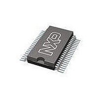
PCF8566TS/1,118 NXP Semiconductors, PCF8566TS/1,118 Datasheet - Page 22

PCF8566TS/1,118
Manufacturer Part Number
PCF8566TS/1,118
Description
IC LCD DISPLAY DVR 24SEG SOT158
Manufacturer
NXP Semiconductors
Datasheet
1.PCF8566T1118.pdf
(48 pages)
Specifications of PCF8566TS/1,118
Package / Case
40-BSOP (0.300", 7.50mm Width)
Display Type
LCD
Configuration
7 Segment + DP, 14 Segment (24 Segment)
Interface
I²C
Current - Supply
30µA
Voltage - Supply
2.5 V ~ 6 V
Operating Temperature
-40°C ~ 85°C
Mounting Type
Surface Mount
Number Of Digits
12
Number Of Segments
24
Maximum Clock Frequency
315 KHz
Operating Supply Voltage
2.5 V to 6 V
Maximum Power Dissipation
400 mW
Attached Touch Screen
No
Maximum Supply Current
90 uA
Lead Free Status / RoHS Status
Lead free / RoHS Compliant
Digits Or Characters
-
Lead Free Status / Rohs Status
Details
NXP Semiconductors
PCF8566_7
Product data sheet
8.1.4 PCF8566 I
8.1.5 Input filter
8.2 I
The PCF8566 acts as an I
transmit data to an I
the acknowledge signals of the selected devices. Device selection depends on the
I
In single device application, the hardware subaddress inputs A0, A1 and A2 are normally
tied to V
A0, A1 and A2 are tied to V
devices with a common I
In the power-saving mode it is possible that the PCF8566 is not able to keep up with the
highest transmission rates when large amounts of display data are transmitted. If this
situation occurs, the PCF8566 forces the SCL line LOW until its internal operations are
completed. This is known as the clock synchronization feature of the I
to slow down fast transmitters. Data loss does not occur.
To enhance noise immunity in electrically adverse environments, RC low-pass filters are
provided on the SDA and SCL lines.
Two I
PCF8566. The least significant bit after the slave address is bit R/W. The PCF8566 is a
write-only device. It will not respond to a read access, so this bit should always be logic 0.
The second bit of the slave address is defined by the level tied at input SA0.
2
2
Fig 15. Acknowledgement on the I
•
C-bus slave address, the transferred command data and the hardware subaddress.
C-bus protocol
A master receiver must signal an end-of-data to the transmitter by not generating an
acknowledge on the last byte that has been clocked out of the slave. In this event, the
master receiver must leave the data line HIGH during the 9th pulse to not
acknowledge. The master will now generate a STOP condition.
2
C-bus 7 bit slave addresses (0111 110 and 0111 111) are reserved for the
by transmitter
SS
data output
by receiver
data output
SCL from
which defines the hardware subaddress 0. In multiple device applications
master
2
C-bus controller
2
condition
START
C-bus master receiver. The only data output from the PCF8566 are
Rev. 07 — 25 February 2009
S
2
C-bus slave address have the same hardware subaddress.
2
C-bus slave receiver. It does not initiate I
SS
or V
DD
1
2
C-bus
using a binary coding scheme so that no two
Universal LCD driver for low multiplex rates
2
not acknowledge
acknowledge
8
2
acknowledgement
C-bus transfers or
clock pulse for
2
PCF8566
C-bus and serves
© NXP B.V. 2009. All rights reserved.
9
mbc602
22 of 48


