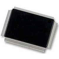
DP83865DVH National Semiconductor, DP83865DVH Datasheet - Page 47

DP83865DVH
Manufacturer Part Number
DP83865DVH
Description
10/100/1000BASE-T TRANSCEIVER, SMD
Manufacturer
National Semiconductor
Specifications of DP83865DVH
Data Rate
1000Mbps
No. Of Ports
1
Ethernet Type
IEEE 802.3u, IEEE 802.3z
Supply Current
430µA
Supply Voltage Range
2.375V To 2.625V, 3.135V To 3.465V
Operating Temperature Range
0°C To +70°C
Interface Type
GMII, MII, RGMII
Rohs Compliant
Yes
Leaded Process Compatible
No
Peak Reflow Compatible (260 C)
No
Lead Free Status / RoHS Status
Lead free / RoHS Compliant
Available stocks
Company
Part Number
Manufacturer
Quantity
Price
Company:
Part Number:
DP83865DVH
Manufacturer:
Texas Instruments
Quantity:
10 000
Company:
Part Number:
DP83865DVH/NOPB
Manufacturer:
NXP
Quantity:
1 000
Company:
Part Number:
DP83865DVH/NOPB
Manufacturer:
Texas Instruments
Quantity:
10 000
3.0 Configuration
See IEEE 802.3ab section 40.6.1.1.2 “Test modes” for
more information on the nature of the test modes.
The DP83865 provides a test clock synchronous to the
IEEE test patterns. The test patterns are output on the MDI
pins of the device and the test clock is output on the
TX_TCLK pin. There are also two support signals available
which are intended to improve the viewability of the test
patterns on an oscilloscope. TX_TRIGGER marks the start
of the test pattern and TX_SYNC_CLK provides and addi-
tional clock. Refer to section “1.6 Device Configuration and
LED Interface” on page 8 for pin numbers.
TX_TCLK, TX_TRIGGER and TX_SYN_CLK must be
enabled through bits 6 and 7 of register AUX_CTRL (0x12)
before they can be used.
3.15 Interrupt
The DP83865 can be configured to generate an interrupt
on pin 3 when changes of internal status occur. The inter-
rupt allows a MAC to act upon the status in the PHY with-
out polling the PHY registers. The interrupt source can be
selected through the interrrupt register set. This register set
consists of:
— Interrupt Status Register (INT_STATUS 0x14)
— Interrupt Mask Register (INT_MASK 0x15)
— Interrupt Clear Register (INT_CLEAR 0x17)
Upon reset, the interrupt is disabled and the interrupt regis-
ters are cleared. Any interrupt source can be enabled in the
INT_MASK register.
The interrupt pin is active low. When the interrupt signal is
asserted it will remain asserted until the corresponding sta-
tus bit is cleared.
The interrupt pin is tri-stated when the interrupt is not
enabled or no interrupt has occured.
The status bits are the sources of the interrupt. These bits
are mapped in INT_STATUS. When the interrupt status bit
is “1”, the interrupt signal is asserted if the corresponding
INT_MASK bit is enabled. An interrupt status bit can be
cleared by writing a “1” to the corresponding bit in
INT_CLEAR. The clear bit returns to “0” automatically after
the interrupt status bit is cleared.
3.16 Low Power Mode / WOL
The GigPHYTER V supports the Wake on LAN (WOL) fea-
ture of a higher layer device. In order to achive the least
possible power consumption the DP83865 must be put in
10BASE-T mode (Half or Full Duplex). In this mode the
device uses a maximum of 146mW of power.
3.17 Power Down Mode
Register BMCR (0x00) bit 11 puts the GigPHYTER V in
Power Down mode. Writing a ‘1’ to this location causes the
DP83865 to deactivate everything but the management
(MDC / MDIO) interface. During this mode the device con-
sumes the least possible power.
3.18 BIST Configuration
The BIST (Built-In Self Test) provides a test interface that
allows to evaluate receive performance and to generate
valid transmit packets. Registers 0x18 (BIST_CNT), 0x19
(BIST_CFG1) and 0x1A (BIST_CFG2) contain the controls
to two distinct BIST functions: Receive BIST and transmit
(Continued)
47
BIST. The receive BIST contains a receive error counter
and receive packet counter and the transmit BIST is used
to generate Ethernet packets.
The BIST can be used to verify operations of all three
speed modes. The speed mode can be established
through auto-negotiation or manual forced mode. The BIST
may also be used in combination with the loopback mode
to verify both the transmit and receive operations of the
physical layer device.
Receive BIST
BIST_CNT displays the upper or lower 16-bit of an internal
32-bit counter. Bit 14 of BIST_CFG2 (bist_cnt_sel) selects
which 16-bit portion is shown while bit 15 of BIST_CFG1
(bist_cnt_type) selects whether the receive packet counter
or the receive error counter is active. The active counter
can be cleared by writing a ‘1’ to bit 14 of BIST_CFG1. The
receive BIST counter is disabled by default and can be
enabled through bit 15 of BIST_CFG2.
The receive BIST can be enabled during normal operation
in order to monitor the incoming data stream. The BIST
operation will not affect the PHY’s performance or behav-
ior.
Transmit BIST
The transmit BIST allows the generation of packets with
pseudo-random (PSR9) or user defined content (bit 10 of
BIST_CFG1),
BIST_CFG1) and variable interframe gap (bit 12 of
BIST_CFG1). Bits 7:0 of BIST_CFG1 contain the content
of the packet as defined by the user if that option has been
chosen.
The number of packets to be sent are specified through bits
13:11 of BIST_CFG2. Setting the enable bit in bit 11 of
BIST_CFG1 starts the transmittal. After the last packet was
sent this bit is automatically cleared. In case the ‘continu-
ous transmit’ has been selected the enable bit must be
cleared in order to stop the stream of packets.
7:0
Bit
15
14
13
12
11
10
Table 47. BIST Configuration 1 Reg (0x19)
Function
Set active counter:
‘1’ = Receive error counter
‘0’ = Receive packet counter
‘1’ = Clear counter
Packet length:
‘1’ = 1514 bytes
‘0’ = 60 bytes
Interframe gap:
‘1’ = 9.6 s
‘0’ = 0.096 s
‘1’ = Enable transmit BIST
Packet type:
‘1’ = PSR9
‘0’ = User defined
User defined packet content.
different
packet
lengths
www.national.com
(bit
13
of


