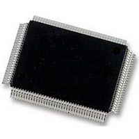
DP83865DVH National Semiconductor, DP83865DVH Datasheet - Page 50

DP83865DVH
Manufacturer Part Number
DP83865DVH
Description
10/100/1000BASE-T TRANSCEIVER, SMD
Manufacturer
National Semiconductor
Specifications of DP83865DVH
Data Rate
1000Mbps
No. Of Ports
1
Ethernet Type
IEEE 802.3u, IEEE 802.3z
Supply Current
430µA
Supply Voltage Range
2.375V To 2.625V, 3.135V To 3.465V
Operating Temperature Range
0°C To +70°C
Interface Type
GMII, MII, RGMII
Rohs Compliant
Yes
Leaded Process Compatible
No
Peak Reflow Compatible (260 C)
No
Lead Free Status / RoHS Status
Lead free / RoHS Compliant
Available stocks
Company
Part Number
Manufacturer
Quantity
Price
Company:
Part Number:
DP83865DVH
Manufacturer:
Texas Instruments
Quantity:
10 000
Company:
Part Number:
DP83865DVH/NOPB
Manufacturer:
NXP
Quantity:
1 000
Company:
Part Number:
DP83865DVH/NOPB
Manufacturer:
Texas Instruments
Quantity:
10 000
www.national.com
4.0 Functional Description
4.1.8 Symbol Sign Scrambler
Symbol Sign Scrambler scrambles the sign of the TA
TB
nary symbol mapping function by either inverting or not
inverting the signs. This is done as follows:
A
B
C
D
The output of this block, namely A
sign scrambled PAM-5 symbols. They are then passed
onto the PMA for further processing.
4.2 1000BASE-T PMA Transmitter
The PMA transmit block shown in Figure 3 contains the fol-
lowing blocks:
— Partial Response Encoder
— DAC and Line Driver
4.2.1 Partial Response Encoder
Partial Response (PR) coding (or shaping) is used on the
PAM-5 coded signals to spectrally shape the transmitted
PAM-5 signal in order to reduce emissions in the critical
frequency band ranging from 30 MHz to 60 MHz. The PR
Z-transform implemented is
The PR coding on the PAM-5 signal results in 17-level PAM-
5 or PAM-17 signal that is used to drive a common
10/100/1000 DAC and line driver. (Without the PR coding
each signal can have 5 levels given by ± 1, ± 0.5 and 0 V. If
all combinations of the 5 levels are used for the present and
previous outputs, then there are 17 unique output levels
when PR coding is used.)
Figure 3 shows the PMA Transmitter and the embedded
PR encoder block with its inputs and outputs. Figure 4
shows the effect on the spectrum of PAM-5 after PR shap-
ing.
4.2.2 DAC and Line Driver
The PAM-17 information from the PR encoder is supplied
to a common 10/100/1000 DAC and line driver that con-
verts digitally encoded data to differential analog voltages.
0.75
n
n
n
n
Input Data
Byte from GMII
TxD
n
= TA
= TB
= TC
= TD
, TC
g
g
n
M
S
+
[7:0]
= 1 + x
= 1 + x
0.25 Z
n
n
LSFR
n
n
n
, and TD
x S
x S
x S
x S
20
13
+ x
+ x
n
n
n
n
1 –
A
33
B
33
C
D
n
n
n
n
n
Scr
input values from the bit-to-symbol qui-
n
[32:0]
Data Scrambler
and Symbol
Sign Scrambler
Word Generator
g(x) = x
3
n
, B
x
8
n
Figure 2. PCS TX Functional Block Diagram
(Continued)
, C
n
Sx
Sy
, and D
n
n
[3:0]
[3:0]
n,
Scrambler
Generator
are the
Bit
n
,
Sc
50
n
[7:0]
4.3 1000BASE-T PMA Receiver
The PMA Receiver (the “Receiver”) consists of several sub
functional blocks that process the four digitized voltage
waveforms representing the received quartet of quinary
PAM-5 symbols. The DSP processing implemented in the
receiver extracts a best estimate of the quartet of quinary
symbols originated by the link partner and delivers them to
the PCS Receiver block for further processing. There are
four separate Receivers, one for each twisted pair.
The main processing sub blocks include:
— Adaptive Equalizer
— Echo and Crosstalk Cancellers
— Automatic Gain Control (AGC)
— Baseline Wander (BLW) Correction
— Slicer
4.3.1 Adaptive Equalizer
The Adaptive Equalizer compensates for the frequency
attenuation characteristics which results from the signal
distortion of the CAT-5 cable. The cable has higher attenu-
ates at the higher frequencies and this attenuation must be
equalized. The Adaptive Equalizer is a digital filter with tap
coefficients continually adapted to minimize the Mean
Square Error (MSE) value of the slicer's error signal output.
Continuous adaptation of the equalizer coefficients means
that the optimum set of coefficients will always be achieved
for maximum specified length or lower quality of cable.
4.3.2 Echo and Crosstalk Cancellers
The Echo and Crosstalk Cancellers cancel the echo and
crosstalk produced while transmitting and receiving simul-
taneously. Echo is produced when the transmitted signal
interferes with the received signal on the same wire pair.
Crosstalk is caused by the transmitted signal appearing on
each of the other three wire pairs interfering with the
receive signal on the fourth wire pair. An Echo and
Crosstalk Canceller is needed for each of the wire pairs.
4.3.3 Automatic Gain Control (AGC)
The Automatic Gain Control acts upon the output of the
Echo and Crosstalk Cancellers to adjust the receiver gain.
Different AGC methods are available within the chip and
the optimum gain is selected based on the operational
state the chip (master, slave, start-up, etc.).
Scrambler and
Convolutional
Encoder
Data
Sd
Sg
n
n
[8:0]
[3:0]
Quinary Symbol
Scrambler
Generator
Mapping
Nibble
Bit-to
Sign
TA
TB
TC
TD
S
S
S
S
n
n
n
n
B
C
A
D
n
n
n
n
n
n
n
n
Scrambler
Symbol
Sign
Sign
Scrambled
PAM-5
Symbols
to PMA
A
B
C
D
n
n
n
n


