DP83865DVH National Semiconductor, DP83865DVH Datasheet - Page 6
DP83865DVH
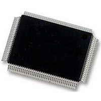
Manufacturer Part Number
DP83865DVH
Description
10/100/1000BASE-T TRANSCEIVER, SMD
Manufacturer
National Semiconductor
Specifications of DP83865DVH
Data Rate
1000Mbps
No. Of Ports
1
Ethernet Type
IEEE 802.3u, IEEE 802.3z
Supply Current
430µA
Supply Voltage Range
2.375V To 2.625V, 3.135V To 3.465V
Operating Temperature Range
0°C To +70°C
Interface Type
GMII, MII, RGMII
Rohs Compliant
Yes
Leaded Process Compatible
No
Peak Reflow Compatible (260 C)
No
Lead Free Status / RoHS Status
Lead free / RoHS Compliant
Available stocks
Company
Part Number
Manufacturer
Quantity
Price
Company:

Part Number:
DP83865DVH
Manufacturer:
Texas Instruments
Quantity:
10 000
Company:
Part Number:
DP83865DVH/NOPB
Manufacturer:
NXP
Quantity:
1 000
Company:
Part Number:
DP83865DVH/NOPB
Manufacturer:
Texas Instruments
Quantity:
10 000


www.national.com
1.0 Pin Description
TXD0/TX0
TXD1/TX1
TXD2/TX2
TXD3/TX3
TXD4
TXD5
TXD6
TXD7
TX_EN/TXEN_ER
GTX_CLK/TCK
TX_ER
RX_CLK
RXD0/RX0
RXD1/RX1
RXD2/RX2
RXD3/RX3
RXD4
RXD5
RXD6
RXD7
RX_ER/RXDV_ER
RX_DV/RCK
Signal Name
Type
O_Z
O_Z
O_Z
O_Z
(Continued)
I
I
I
I
PQFP
Pin #
76
75
72
71
68
67
66
65
62
79
61
57
56
55
52
51
50
47
46
45
41
44
TRANSMIT DATA: These signals carry 4B data nibbles (TXD[3:0]) during 10
Mbps and 100 Mbps MII mode, 4-bit data (TX[3:0]) in RGMII mode, and 8-bit
data (TXD[7:0]) in 1000 Mbps GMII mode. They are synchronous to the trans-
mit clocks (TX_CLK, TCK, GTX_CLK).
Transmit data is input to PHY. In MII or GMII mode, the transmit data is en-
abled by TX_EN. In RGMII mode, the transmit data is enabled by TXEN_ER.
TRANSMIT ENABLE or TRANSMIT ENABLE/ERROR: In MII or GMII mode,
it is an active high input sourced from MAC layer to indicate transmission data
is available on the TXD.
In RGMII mode, it combines the transmit enable and the transmit error signals
of GMII mode using both clock edges.
GMII and RGMII TRANSMIT CLOCK: This continuous clock signal is sourced
from the MAC layer to the PHY. Nominal frequency is 125 MHz.
TRANSMIT ERROR: It is an active high input used in MII mode and GMII
mode forcing the PHY to transmit invalid symbols. The TX_ER signal is syn-
chronous to the transmit clocks (TX_CLK or GTX_CLK).
In MII 4B nibble mode, assertion of Transmit Error by the controller causes the
PHY to issue invalid symbols followed by Halt (H) symbols until deassertion oc-
curs.
In GMII mode, assertion causes the PHY to emit one or more code-groups that
are invalid data or delimiter in the transmitted frame.
This signal is not used in the RGMII mode.
RECEIVE CLOCK: Provides the recovered receive clocks for different modes
of operation:
2.5 MHz in 10 Mbps mode.
25 MHz in 100 Mbps mode.
125 MHz in 1000 Mps GMII mode.
This pin is not used in the RGMII mode.
RECEIVE DATA: These signals carry 4-bit data nibbles (RXD[3:0]) during 10
Mbps and 100 Mbps MII mode and 8-bit data bytes (RXD[7:0]) in 1000 Mbps
GMII mode. RXD is synchronous to the receive clock (RX_CLK). Receive data
is souirced from the PHY to the MAC layer.
Receive data RX[3:0] is used in RGMII mode. The data is synchronous to the
RGMII receive clock (RCK). The receive data available (RXDV_EN) indicates
valid received data to the MAC layer.
RECEIVE ERROR or RECEIVE DATA AVAILABLE/ERROR: In 10 Mbps,
100 Mbps and 1000 Mbps mode this active high output indicates that the PHY
has detected a Receive Error. The RX_ER signal is synchronous with the re-
ceive clock (RX_CLK).
In RGMII mode, the receive data available and receive error is combined
(RXDV_ER) using both rising and falling edges of the receive clock (RCK).
RECEIVE DATA VALID or RECEIVE CLOCK: In MII and GMII modes, it is as-
serted high to indicate that valid data is present on the corresponding RXD[3:0]
in MII mode and RXD[7:0] in GMII mode.
In RGMII mode, this pin is the recovered receive clock (125MHz).
6
Description
Related parts for DP83865DVH
Image
Part Number
Description
Manufacturer
Datasheet
Request
R

Part Number:
Description:
BOARD EVALUATION DP83865
Manufacturer:
National Semiconductor
Datasheet:
Part Number:
Description:
National Semiconductor [8-Bit D/A Converter]
Manufacturer:
National Semiconductor
Datasheet:
Part Number:
Description:
National Semiconductor [Media Coprocessor]
Manufacturer:
National Semiconductor
Datasheet:
Part Number:
Description:
Digitally Controlled Tone and Volume Circuit with Stereo Audio Power Amplifier, Microphone Preamp Stage and National 3D Sound
Manufacturer:
National Semiconductor
Datasheet:
Part Number:
Description:
Digitally Controlled Tone and Volume Circuit with Stereo Audio Power Amplifier, Microphone Preamp Stage and National 3D Sound
Manufacturer:
National Semiconductor
Datasheet:
Part Number:
Description:
AC97 Rev 2 Codec with Sample Rate Conversion and National 3D Sound
Manufacturer:
National Semiconductor
Part Number:
Description:
Manufacturer:
National Semiconductor
Datasheet:
Part Number:
Description:
Manufacturer:
National Semiconductor
Datasheet:
Part Number:
Description:
General Purpose, Low Voltage, Low Power, Rail-to-Rail Output Operational Amplifiers
Manufacturer:
National Semiconductor
Datasheet:
Part Number:
Description:
8-bit 20 MSPS flash A/D converter.
Manufacturer:
National Semiconductor
Datasheet:
Part Number:
Description:
Low Noise Quad Operational Amplifier
Manufacturer:
National Semiconductor
Datasheet:
Part Number:
Description:
Quad Differential Line Receivers
Manufacturer:
National Semiconductor
Datasheet:
Part Number:
Description:
Quad High Speed Trapezoidal? Bus Transceiver
Manufacturer:
National Semiconductor
Datasheet:
Part Number:
Description:
Dual Line Receiver
Manufacturer:
National Semiconductor
Datasheet: