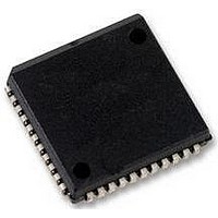
SC16C2552BIA44 NXP Semiconductors, SC16C2552BIA44 Datasheet - Page 7

SC16C2552BIA44
Manufacturer Part Number
SC16C2552BIA44
Description
UART, 2 CH, 16BYTE FIFO, 16C2552
Manufacturer
NXP Semiconductors
Datasheet
1.SC16C2552BIA44.pdf
(38 pages)
Specifications of SC16C2552BIA44
No. Of Channels
2
Data Rate
5Mbps
Supply Voltage Range
2.25V To 5.5V
Operating Temperature Range
-40°C To +85°C
Digital Ic Case Style
PLCC
No. Of Pins
44
Svhc
No SVHC (18-Jun-2010)
Operating
RoHS Compliant
Uart Features
Independent Transmit & Receive UART Control, Multi-Function Output, Modem Control Functions
Rohs Compliant
Yes
Available stocks
Company
Part Number
Manufacturer
Quantity
Price
Part Number:
SC16C2552BIA44
Manufacturer:
NXP/恩智浦
Quantity:
20 000
Company:
Part Number:
SC16C2552BIA44,529
Manufacturer:
NXP Semiconductors
Quantity:
10 000
NXP Semiconductors
SC16C2552B_3
Product data sheet
6.2 Internal registers
6.3 FIFO operation
6.4 Time-out interrupts
The SC16C2552B provides two sets of internal registers (A and B) consisting of
13 registers each for monitoring and controlling the functions of each channel of the
UART. These registers are shown in
registers (THR/RHR), interrupt status and control registers (IER/ISR), a FIFO control
register (FCR), line status and control registers (LCR/LSR), modem status and control
registers (MCR/MSR), programmable data rate (clock) control registers (DLL/DLM), a
user accessible scratchpad register (SPR), and an Alternate Function Register (AFR).
Table 4.
[1]
The 16 byte transmit and receive data FIFOs are enabled by the FIFO Control Register
(FCR) bit 0. The user can set the receive trigger level via FCR[7:6], but not the transmit
trigger level. The receiver FIFO section includes a time-out function to ensure data is
delivered to the external CPU. A time-out interrupt is generated whenever the Receive
Holding Register (RHR) has not been read following the loading of a character, or the
receive trigger interrupt is generated when RX FIFO level is equal to the program RX
trigger value.
The interrupts are enabled by IER[3:0]. Care must be taken when handling these
interrupts. Following a reset, if the transmitter interrupt is enabled, the SC16C2552B will
issue an interrupt to indicate that the Transmit Holding Register is empty. The ISR register
provides the current singular highest priority interrupt only. A condition can exist where a
higher priority interrupt may mask the lower priority interrupt(s). Only after servicing the
higher pending interrupt will the lower priority interrupt(s) be reflected in the status
register. Servicing the interrupt without investigating further interrupt conditions can result
in data errors.
A2
General register set (THR/RHR, IER/ISR, MCR/MSR, FCR, LCR/LSR, SPR)
0
0
0
0
1
1
1
1
Baud rate register set (DLL/DLM, AFR)
0
0
0
The baud rate register and AFR register sets are accessible only when CS is a logic 0 and LCR[7] is a
logic 1 for the register set (A/B) being accessed.
A1
0
0
1
1
0
0
1
1
0
0
1
Internal registers decoding
A0
0
1
0
1
0
1
0
1
0
1
0
5 V, 3.3 V and 2.5 V dual UART, 5 Mbit/s (max.), with 16-byte FIFOs
Rev. 03 — 12 February 2009
Read mode
Receive Holding Register
Interrupt Enable Register
Interrupt Status Register
Line Control Register
Modem Control Register
Line Status Register
Modem Status Register
Scratchpad Register
LSB of Divisor Latch
MSB of Divisor Latch
Alternate Function Register
Table
[1]
4. The UART registers function as data holding
Write mode
Transmit Holding Register
Interrupt Enable Register
FIFO Control Register
Line Control Register
Modem Control Register
n/a
n/a
Scratchpad Register
LSB of Divisor Latch
MSB of Divisor Latch
Alternate Function Register
SC16C2552B
© NXP B.V. 2009. All rights reserved.
7 of 38


