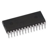
DSPIC30F2010-30I/SPG Microchip Technology, DSPIC30F2010-30I/SPG Datasheet - Page 105

DSPIC30F2010-30I/SPG
Manufacturer Part Number
DSPIC30F2010-30I/SPG
Description
16BIT 30MIPS DSPIC, 30F2010, DIP28
Manufacturer
Microchip Technology
Series
DsPIC30Fr
Datasheet
1.DSPIC30F2010-30ISPG.pdf
(244 pages)
Specifications of DSPIC30F2010-30I/SPG
Core Frequency
30MHz
Embedded Interface Type
I2C, SPI, UART
No. Of I/o's
20
Flash Memory Size
12KB
Supply Voltage Range
2.5V To 5.5V
Operating Temperature Range
-40°C To
Lead Free Status / RoHS Status
Lead free / RoHS Compliant
- Current page: 105 of 244
- Download datasheet (7Mb)
15.1.5
The input clock to PTMR (F
options of 1:1, 1:4, 1:16, or 1:64, selected by control
bits PTCKPS<1:0> in the PTCON SFR. The prescaler
counter is cleared when any of the following occurs:
• a write to the PTMR register
• a write to the PTCON register
• any device Reset
The PTMR register is not cleared when PTCON is
written.
15.1.6
The match output of PTMR can optionally be post-
scaled through a 4-bit postscaler (which gives a 1:1 to
1:16 scaling).
The postscaler counter is cleared when any of the
following occurs:
• a write to the PTMR register
• a write to the PTCON register
• any device Reset
The PTMR register is not cleared when PTCON is written.
15.2
PTPER is a 15-bit register and is used to set the count-
ing period for the PWM time base. PTPER is a double
buffered register. The PTPER buffer contents are
loaded into the PTPER register at the following instants:
• Free Running and Single Shot modes: When the
• Up/Down Counting modes: When the PTMR
The value held in the PTPER buffer is automatically
loaded into the PTPER register when the PWM time
base is disabled (PTEN = 0).
The
Equation 15-1:
EQUATION 15-1:
If the PWM time base is configured for one of the Up/
Down Count modes, the PWM period will be twice the
value provided by Equation 15-1.
2004 Microchip Technology Inc.
PTMR register is reset to zero after a match with
the PTPER register.
register is zero.
PWM
PWM Period
T
PWM
PWM TIME BASE PRESCALER
PWM TIME BASE POSTSCALER
period
=
(PTMR Prescale Value)
T
PWM PERIOD
CY
can
•
(PTPER + 1)
be
OSC
determined
/4), has prescaler
Advance Information
using
The maximum resolution (in bits) for a given device
oscillator and PWM frequency can be determined using
Equation 15-2:
EQUATION 15-2:
15.3
Edge aligned PWM signals are produced by the module
when the PWM time base is in the Free Running or Sin-
gle Shot mode. For edge aligned PWM outputs, the out-
put has a period specified by the value in PTPER and a
duty cycle specified by the appropriate duty cycle regis-
ter (see Figure 15-3). The PWM output is driven active
at the beginning of the period (PTMR = 0) and is driven
inactive when the value in the duty cycle register
matches PTMR.
If the value in a particular duty cycle register is zero,
then the output on the corresponding PWM pin will be
inactive for the entire PWM period. In addition, the out-
put on the PWM pin will be active for the entire PWM
period if the value in the duty cycle register is greater
than the value held in the PTPER register.
FIGURE 15-3:
15.4
Center aligned PWM signals are produced by the mod-
ule when the PWM time base is configured in an Up/
Down Counting mode (see Figure 15-4).
The PWM compare output is driven to the active state
when the value of the duty cycle register matches the
value of PTMR and the PWM time base is counting
downwards (PTDIR = 1). The PWM compare output is
driven to the inactive state when the PWM time base is
counting upwards (PTDIR = 0) and the value in the
PTMR register matches the duty cycle value.
PTPER
0
Resolution =
Edge Aligned PWM
Center Aligned PWM
PTMR
Value
Duty Cycle
Period
PWM RESOLUTION
EDGE ALIGNED PWM
log (2
New Duty Cycle Latched
dsPIC30F
log (2)
•
T
PWM
DS70082E-page 103
/ T
CY
)
Related parts for DSPIC30F2010-30I/SPG
Image
Part Number
Description
Manufacturer
Datasheet
Request
R

Part Number:
Description:
IC DSPIC MCU/DSP 12K 28DIP
Manufacturer:
Microchip Technology
Datasheet:

Part Number:
Description:
IC DSPIC MCU/DSP 12K 28SOIC
Manufacturer:
Microchip Technology
Datasheet:

Part Number:
Description:
IC,DSP,16-BIT,CMOS,SOP,28PIN,PLASTIC
Manufacturer:
Microchip Technology
Datasheet:

Part Number:
Description:
IC DSPIC MCU/DSP 12K 28SOIC
Manufacturer:
Microchip Technology
Datasheet:

Part Number:
Description:
IC DSPIC MCU/DSP 12K 28QFN
Manufacturer:
Microchip Technology
Datasheet:

Part Number:
Description:
IC DSPIC MCU/DSP 12K 28QFN
Manufacturer:
Microchip Technology
Datasheet:

Part Number:
Description:
IC DSPIC MCU/DSP 12K 28DIP
Manufacturer:
Microchip Technology
Datasheet:

Part Number:
Description:
IC DSPIC MCU/DSP 12K 28SOIC
Manufacturer:
Microchip Technology
Datasheet:

Part Number:
Description:
IC DSPIC MCU/DSP 12K 28DIP
Manufacturer:
Microchip Technology
Datasheet:

Part Number:
Description:
IC DSPIC MCU/DSP 12K 28SOIC
Manufacturer:
Microchip Technology

Part Number:
Description:
IC DSPIC MCU/DSP 12K 28QFN
Manufacturer:
Microchip Technology

Part Number:
Description:
IC DSPIC MCU/DSP 12K 28DIP
Manufacturer:
Microchip Technology

Part Number:
Description:
IC,DSP,16-BIT,CMOS,LLCC,28PIN,PLASTIC
Manufacturer:
Microchip Technology
Datasheet:

Part Number:
Description:
Digital Signal Processors & Controllers - DSP, DSC
Manufacturer:
Microchip Technology

Part Number:
Description:
Digital Signal Processors & Controllers - DSP, DSC 16 Bit MCU/DSP 28LD 20M 12KB FL
Manufacturer:
Microchip Technology


