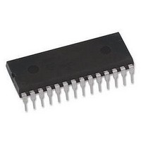
DSPIC30F2010-30I/SPG Microchip Technology, DSPIC30F2010-30I/SPG Datasheet - Page 63

DSPIC30F2010-30I/SPG
Manufacturer Part Number
DSPIC30F2010-30I/SPG
Description
16BIT 30MIPS DSPIC, 30F2010, DIP28
Manufacturer
Microchip Technology
Series
DsPIC30Fr
Datasheet
1.DSPIC30F2010-30ISPG.pdf
(244 pages)
Specifications of DSPIC30F2010-30I/SPG
Core Frequency
30MHz
Embedded Interface Type
I2C, SPI, UART
No. Of I/o's
20
Flash Memory Size
12KB
Supply Voltage Range
2.5V To 5.5V
Operating Temperature Range
-40°C To
Lead Free Status / RoHS Status
Lead free / RoHS Compliant
- Current page: 63 of 244
- Download datasheet (7Mb)
7.0
The Data EEPROM Memory is readable and writable
during normal operation over the entire V
data EEPROM memory is directly mapped in the
program memory address space.
The four SFRs used to read and write the program
Flash memory are used to access data EEPROM
memory, as well. As described in Section 4.0, these
registers are:
• NVMCON
• NVMADR
• NVMADRU
• NVMKEY
The EEPROM data memory allows read and write of
single words and 16-word blocks. When interfacing to
data memory, NVMADR, in conjunction with the
NVMADRU register, is used to address the EEPROM
location being accessed. TBLRDL and TBLWTL instruc-
tions are used to read and write data EEPROM. The
dsPIC30F devices have up to 8 Kbytes (4K words) of
data EEPROM, with an address range from 0x7FF000
to 0x7FFFFE.
A word write operation should be preceded by an erase
of the corresponding memory location(s). The write typ-
ically requires 2 ms to complete, but the write time will
vary with voltage and temperature.
A program or erase operation on the data EEPROM
does not stop the instruction flow. The user is respon-
sible for waiting for the appropriate duration of time
before initiating another data EEPROM write/erase
operation. Attempting to read the data EEPROM while
a programming or erase operation is in progress results
in unspecified data.
2004 Microchip Technology Inc.
Note: This data sheet summarizes the features of this family of dsPIC30F devices and is not intended to be a complete reference
source. For complete information on the CPU, peripherals, register descriptions and general device functionality, please refer to the
dsPIC30F Family Reference Manual (DS70046). For complete information on the device instruction set and programming, please
refer to the dsPIC30F Programmer’s Reference Manual (DS70030). For device pinouts and electrical specifications, please refer to
the specific data sheet for the device that will be used in your design.
DATA EEPROM MEMORY
DD
range. The
Advance Information
Control bit WR initiates write operations, similar to pro-
gram Flash writes. This bit cannot be cleared, only set,
in software. This bit is cleared in hardware at the com-
pletion of the write operation. The inability to clear the
WR bit in software prevents the accidental or
premature termination of a write operation.
The WREN bit, when set, will allow a write operation.
On power-up, the WREN bit is clear. The WRERR bit is
set when a write operation is interrupted by a MCLR
Reset, or a WDT Time-out Reset, during normal oper-
ation. In these situations, following Reset, the user can
check the WRERR bit and rewrite the location. The
address register NVMADR remains unchanged.
7.1
A TBLRD instruction reads a word at the current pro-
gram word address. This example uses W0 as a
pointer to data EEPROM. The result is placed in
register W4, as shown in Example 7-1.
EXAMPLE 7-1:
MOV
MOV
MOV
TBLRDL [ W0 ], W4
Note:
Reading the Data EEPROM
#LOW_ADDR_WORD,W0
#HIGH_ADDR_WORD,W1
W1
Interrupt flag bit NVMIF in the IFS0 regis-
ter is set when write is complete. It must be
cleared in software.
,
TBLPAG
DATA EEPROM READ
dsPIC30F
; Init Pointer
; read data EEPROM
DS70082E-page 61
Related parts for DSPIC30F2010-30I/SPG
Image
Part Number
Description
Manufacturer
Datasheet
Request
R

Part Number:
Description:
IC DSPIC MCU/DSP 12K 28DIP
Manufacturer:
Microchip Technology
Datasheet:

Part Number:
Description:
IC DSPIC MCU/DSP 12K 28SOIC
Manufacturer:
Microchip Technology
Datasheet:

Part Number:
Description:
IC,DSP,16-BIT,CMOS,SOP,28PIN,PLASTIC
Manufacturer:
Microchip Technology
Datasheet:

Part Number:
Description:
IC DSPIC MCU/DSP 12K 28SOIC
Manufacturer:
Microchip Technology
Datasheet:

Part Number:
Description:
IC DSPIC MCU/DSP 12K 28QFN
Manufacturer:
Microchip Technology
Datasheet:

Part Number:
Description:
IC DSPIC MCU/DSP 12K 28QFN
Manufacturer:
Microchip Technology
Datasheet:

Part Number:
Description:
IC DSPIC MCU/DSP 12K 28DIP
Manufacturer:
Microchip Technology
Datasheet:

Part Number:
Description:
IC DSPIC MCU/DSP 12K 28SOIC
Manufacturer:
Microchip Technology
Datasheet:

Part Number:
Description:
IC DSPIC MCU/DSP 12K 28DIP
Manufacturer:
Microchip Technology
Datasheet:

Part Number:
Description:
IC DSPIC MCU/DSP 12K 28SOIC
Manufacturer:
Microchip Technology

Part Number:
Description:
IC DSPIC MCU/DSP 12K 28QFN
Manufacturer:
Microchip Technology

Part Number:
Description:
IC DSPIC MCU/DSP 12K 28DIP
Manufacturer:
Microchip Technology

Part Number:
Description:
IC,DSP,16-BIT,CMOS,LLCC,28PIN,PLASTIC
Manufacturer:
Microchip Technology
Datasheet:

Part Number:
Description:
Digital Signal Processors & Controllers - DSP, DSC
Manufacturer:
Microchip Technology

Part Number:
Description:
Digital Signal Processors & Controllers - DSP, DSC 16 Bit MCU/DSP 28LD 20M 12KB FL
Manufacturer:
Microchip Technology


