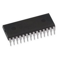
DSPIC30F2010-30I/SPG Microchip Technology, DSPIC30F2010-30I/SPG Datasheet - Page 156

DSPIC30F2010-30I/SPG
Manufacturer Part Number
DSPIC30F2010-30I/SPG
Description
16BIT 30MIPS DSPIC, 30F2010, DIP28
Manufacturer
Microchip Technology
Series
DsPIC30Fr
Datasheet
1.DSPIC30F2010-30ISPG.pdf
(244 pages)
Specifications of DSPIC30F2010-30I/SPG
Core Frequency
30MHz
Embedded Interface Type
I2C, SPI, UART
No. Of I/o's
20
Flash Memory Size
12KB
Supply Voltage Range
2.5V To 5.5V
Operating Temperature Range
-40°C To
Lead Free Status / RoHS Status
Lead free / RoHS Compliant
- Current page: 156 of 244
- Download datasheet (7Mb)
dsPIC30F
The OSCCON register holds the CONTROL and
STATUS bits related to clock switching.
• COSC<1:0>: Read only status bits always reflect
• NOSC<1:0>: Control bits which are written to
• LOCK: The LOCK status bit indicates a PLL lock.
• CF: Read only status bit indicating if a clock fail
• OSWEN: Control bit changes from a ‘0’ to a ‘1’
If configuration bits FCKSM<1:0> = 1x, then the clock
switching and fail-safe clock monitor functions are
disabled. This is the default configuration bit setting.
If clock switching is disabled, then the FOS<1:0> and
FPR<3:0> bits directly control the oscillator selection
and the COSC<1:0> bits do not control the clock
selection. However, these bits will reflect the clock
source selection.
DS70082E-page 154
the current oscillator group in effect.
indicate the new oscillator group of choice.
- On POR and BOR, COSC<1:0> and
detect has occurred.
when a clock transition sequence is initiated.
Clearing the OSWEN control bit will abort a clock
transition in progress (used for hang-up
situations).
Note:
NOSC<1:0> are both loaded with the
Configuration bit values FOS<1:0>.
The application should not attempt to
switch to a clock of frequency lower than
100 KHz when the fail-safe clock monitor is
enabled. If such clock switching is
performed, the device may generate an
oscillator fail trap and switch to the Fast RC
oscillator.
Advance Information
21.2.8
A write to the OSCCON register is intentionally made
difficult because it controls clock switching and clock
scaling.
To write to the OSCCON low byte, the following code
sequence must be executed without any other
instructions in between:
• Byte Write “0x46” to OSCCON low
• Byte Write “0x57” to OSCCON low
Byte Write is allowed for one instruction cycle. Write the
desired value or use bit manipulation instruction.
To write to the OSCCON high byte, the following
instructions must be executed without any other
instructions in between:
• Byte Write “0x78” to OSCCON high
• Byte Write “0x9A” to OSCCON high
Byte Write is allowed for one instruction cycle. Write the
desired value or use bit manipulation instruction.
PROTECTION AGAINST
ACCIDENTAL WRITES TO OSCCON
2004 Microchip Technology Inc.
Related parts for DSPIC30F2010-30I/SPG
Image
Part Number
Description
Manufacturer
Datasheet
Request
R

Part Number:
Description:
IC DSPIC MCU/DSP 12K 28DIP
Manufacturer:
Microchip Technology
Datasheet:

Part Number:
Description:
IC DSPIC MCU/DSP 12K 28SOIC
Manufacturer:
Microchip Technology
Datasheet:

Part Number:
Description:
IC,DSP,16-BIT,CMOS,SOP,28PIN,PLASTIC
Manufacturer:
Microchip Technology
Datasheet:

Part Number:
Description:
IC DSPIC MCU/DSP 12K 28SOIC
Manufacturer:
Microchip Technology
Datasheet:

Part Number:
Description:
IC DSPIC MCU/DSP 12K 28QFN
Manufacturer:
Microchip Technology
Datasheet:

Part Number:
Description:
IC DSPIC MCU/DSP 12K 28QFN
Manufacturer:
Microchip Technology
Datasheet:

Part Number:
Description:
IC DSPIC MCU/DSP 12K 28DIP
Manufacturer:
Microchip Technology
Datasheet:

Part Number:
Description:
IC DSPIC MCU/DSP 12K 28SOIC
Manufacturer:
Microchip Technology
Datasheet:

Part Number:
Description:
IC DSPIC MCU/DSP 12K 28DIP
Manufacturer:
Microchip Technology
Datasheet:

Part Number:
Description:
IC DSPIC MCU/DSP 12K 28SOIC
Manufacturer:
Microchip Technology

Part Number:
Description:
IC DSPIC MCU/DSP 12K 28QFN
Manufacturer:
Microchip Technology

Part Number:
Description:
IC DSPIC MCU/DSP 12K 28DIP
Manufacturer:
Microchip Technology

Part Number:
Description:
IC,DSP,16-BIT,CMOS,LLCC,28PIN,PLASTIC
Manufacturer:
Microchip Technology
Datasheet:

Part Number:
Description:
Digital Signal Processors & Controllers - DSP, DSC
Manufacturer:
Microchip Technology

Part Number:
Description:
Digital Signal Processors & Controllers - DSP, DSC 16 Bit MCU/DSP 28LD 20M 12KB FL
Manufacturer:
Microchip Technology


