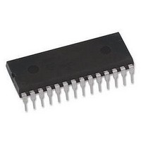
DSPIC30F2010-30I/SPG Microchip Technology, DSPIC30F2010-30I/SPG Datasheet - Page 52

DSPIC30F2010-30I/SPG
Manufacturer Part Number
DSPIC30F2010-30I/SPG
Description
16BIT 30MIPS DSPIC, 30F2010, DIP28
Manufacturer
Microchip Technology
Series
DsPIC30Fr
Datasheet
1.DSPIC30F2010-30ISPG.pdf
(244 pages)
Specifications of DSPIC30F2010-30I/SPG
Core Frequency
30MHz
Embedded Interface Type
I2C, SPI, UART
No. Of I/o's
20
Flash Memory Size
12KB
Supply Voltage Range
2.5V To 5.5V
Operating Temperature Range
-40°C To
Lead Free Status / RoHS Status
Lead free / RoHS Compliant
- Current page: 52 of 244
- Download datasheet (7Mb)
dsPIC30F
5.1
The user assignable Interrupt Priority (IP<2:0>) bits for
each individual interrupt source are located in the LS 3-
bits of each nibble, within the IPCx register(s). Bit 3 of
each nibble is not used and is read as a ‘0’. These bits
define the priority level assigned to a particular interrupt
by the user.
Since more than one interrupt request source may be
assigned to a specific user specified priority level, a
means is provided to assign priority within a given level.
This method is called “Natural Order Priority”.
Table 5-1 lists the interrupt numbers and interrupt
sources for the dsPIC devices and their associated
vector numbers.
The ability for the user to assign every interrupt to one
of seven priority levels implies that the user can assign
a very high overall priority level to an interrupt with a
low natural order priority. For example, the PLVD (Low
Voltage Detect) can be given a priority of 7. The INT0
(external interrupt 0) may be assigned to priority level
1, thus giving it a very low effective priority.
DS70082E-page 50
Note:
Note 1: The natural order priority scheme has 0
2: The natural order priority number is the
Interrupt Priority
The user selectable priority levels start at
0, as the lowest priority, and level 7, as the
highest priority.
as the highest priority and 53 as the
lowest priority.
same as the INT number.
Advance Information
TABLE 5-1:
Highest Natural Order Priority
Lowest Natural Order Priority
Number
45-53
INT
10
11
12
13
14
15
16
17
18
19
20
21
22
23
24
25
26
27
28
29
30
31
32
33
34
35
36
37
38
39
40
41
42
43
44
0
1
2
3
4
5
6
7
8
9
Numbe
Vector
53-61
10
12
13
14
15
16
17
18
19
20
21
22
23
24
25
26
27
28
29
30
31
32
33
34
35
36
37
38
39
40
41
42
43
44
45
46
47
48
49
50
51
52
11
8
9
r
NATURAL ORDER PRIORITY
INT0 - External Interrupt 0
IC1 - Input Capture 1
OC1 - Output Compare 1
T1 - Timer 1
IC2 - Input Capture 2
OC2 - Output Compare 2
T2 - Timer 2
T3 - Timer 3
SPI1
U1RX - UART1 Receiver
U1TX - UART1 Transmitter
ADC - ADC Convert Done
NVM - NVM Write Complete
SI2C - I
MI2C - I
Input Change Interrupt
INT1 - External Interrupt 1
IC7 - Input Capture 7
IC8 - Input Capture 8
OC3 - Output Compare 3
OC4 - Output Compare 4
T4 - Timer 4
T5 - Timer 5
INT2 - External Interrupt 2
U2RX - UART2 Receiver
U2TX - UART2 Transmitter
SPI2
C1 - Combined IRQ for CAN1
IC3 - Input Capture 3
IC4 - Input Capture 4
IC5 - Input Capture 5
IC6 - Input Capture 6
OC5 - Output Compare 5
OC6 - Output Compare 6
OC7 - Output Compare 7
OC8 - Output Compare 8
INT3 - External Interrupt 3
INT4 - External Interrupt 4
C2 - Combined IRQ for CAN2
PWM - PWM Period Match
QEI - QEI Interrupt
Reserved
LVD - Low Voltage Detect
FLTA - PWM Fault A
FLTB - PWM Fault B
Reserved
2004 Microchip Technology Inc.
Interrupt Source
2
2
C Slave Interrupt
C Master Interrupt
Related parts for DSPIC30F2010-30I/SPG
Image
Part Number
Description
Manufacturer
Datasheet
Request
R

Part Number:
Description:
IC DSPIC MCU/DSP 12K 28DIP
Manufacturer:
Microchip Technology
Datasheet:

Part Number:
Description:
IC DSPIC MCU/DSP 12K 28SOIC
Manufacturer:
Microchip Technology
Datasheet:

Part Number:
Description:
IC,DSP,16-BIT,CMOS,SOP,28PIN,PLASTIC
Manufacturer:
Microchip Technology
Datasheet:

Part Number:
Description:
IC DSPIC MCU/DSP 12K 28SOIC
Manufacturer:
Microchip Technology
Datasheet:

Part Number:
Description:
IC DSPIC MCU/DSP 12K 28QFN
Manufacturer:
Microchip Technology
Datasheet:

Part Number:
Description:
IC DSPIC MCU/DSP 12K 28QFN
Manufacturer:
Microchip Technology
Datasheet:

Part Number:
Description:
IC DSPIC MCU/DSP 12K 28DIP
Manufacturer:
Microchip Technology
Datasheet:

Part Number:
Description:
IC DSPIC MCU/DSP 12K 28SOIC
Manufacturer:
Microchip Technology
Datasheet:

Part Number:
Description:
IC DSPIC MCU/DSP 12K 28DIP
Manufacturer:
Microchip Technology
Datasheet:

Part Number:
Description:
IC DSPIC MCU/DSP 12K 28SOIC
Manufacturer:
Microchip Technology

Part Number:
Description:
IC DSPIC MCU/DSP 12K 28QFN
Manufacturer:
Microchip Technology

Part Number:
Description:
IC DSPIC MCU/DSP 12K 28DIP
Manufacturer:
Microchip Technology

Part Number:
Description:
IC,DSP,16-BIT,CMOS,LLCC,28PIN,PLASTIC
Manufacturer:
Microchip Technology
Datasheet:

Part Number:
Description:
Digital Signal Processors & Controllers - DSP, DSC
Manufacturer:
Microchip Technology

Part Number:
Description:
Digital Signal Processors & Controllers - DSP, DSC 16 Bit MCU/DSP 28LD 20M 12KB FL
Manufacturer:
Microchip Technology


