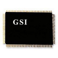
GS840Z36AGT-166 GSI TECHNOLOGY, GS840Z36AGT-166 Datasheet - Page 14

GS840Z36AGT-166
Manufacturer Part Number
GS840Z36AGT-166
Description
IC, 4MB SYNCH NBT SRAM 1M X 36, 840
Manufacturer
GSI TECHNOLOGY
Datasheet
1.GS840Z36AGT-166.pdf
(24 pages)
Specifications of GS840Z36AGT-166
Memory Size
4Mbit
Clock Frequency
166MHz
Access Time
8.5ns
Supply Voltage Range
2.3V To 2.7V, 3V To 3.6V
Memory Case Style
TQFP
No. Of Pins
100
Operating Temperature Range
0°C To +70°C
Memory Configuration
128K X 36
Rohs Compliant
Yes
Lead Free Status / RoHS Status
Lead free / RoHS Compliant
Available stocks
Company
Part Number
Manufacturer
Quantity
Price
V
V
Recommended Operating Temperatures
Rev: 1.03 11/2004
Specifications cited are subject to change without notice. For latest documentation see http://www.gsitechnology.com.
Notes:
1.
2.
3.
Notes:
1.
2.
3.
Notes:
1.
2.
Ambient Temperature (Commercial Range Versions)
DDQ3
DDQ2
Ambient Temperature (Industrial Range Versions)
The part numbers of Industrial Temperature Range versions end the character “I”. Unless otherwise noted, all performance specifica-
tions quoted are evaluated for worst case in the temperature range marked on the device.
Input Under/overshoot voltage must be –2 V > Vi < V
V
The part numbers of Industrial Temperature Range versions end the character “I”. Unless otherwise noted, all performance specifica-
tions quoted are evaluated for worst case in the temperature range marked on the device.
Input Under/overshoot voltage must be –2 V > Vi < V
V
The part numbers of Industrial Temperature Range versions end the character “I”. Unless otherwise noted, all performance specifica-
tions quoted are evaluated for worst case in the temperature range marked on the device.
Input Under/overshoot voltage must be –2 V > Vi < V
IHQ
IHQ
Range Logic Levels
Range Logic Levels
(max) is voltage on V
(max) is voltage on V
V
V
V
V
DDQ
DDQ
DDQ
DDQ
V
V
V
V
DD
DD
DD
DD
I/O Input High Voltage
I/O Input High Voltage
I/O Input Low Voltage
I/O Input Low Voltage
Input High Voltage
Input High Voltage
Parameter
Input Low Voltage
Parameter
Input Low Voltage
Parameter
DDQ
DDQ
pins plus 0.3 V.
pins plus 0.3 V.
Symbol
Symbol
Symbol
DDn
DDn
DDn
V
V
V
V
V
V
V
V
T
T
IHQ
IHQ
ILQ
ILQ
14/24
+2 V not to exceed 4.6 V maximum, with a pulse width not to exceed 20% tKC.
+2 V not to exceed 4.6 V maximum, with a pulse width not to exceed 20% tKC.
+2 V not to exceed 4.6 V maximum, with a pulse width not to exceed 20% tKC.
IH
IL
IH
IL
A
A
0.6*V
0.6*V
Min.
Min.
Min.
–0.3
–0.3
–0.3
–0.3
–40
2.0
2.0
0
DD
DD
Typ.
Typ.
Typ.
—
—
—
—
—
—
—
—
25
25
GS840Z18/36AT-180/166/150/100
V
V
V
V
DDQ
DDQ
0.3*V
0.3*V
DD
DD
Max.
Max.
Max.
0.8
0.8
70
85
+ 0.3
+ 0.3
+ 0.3
+ 0.3
DD
DD
Unit
Unit
Unit
°C
°C
V
V
V
V
V
V
V
V
© 2001, GSI Technology
Notes
Notes
Notes
1,3
1,3
1,3
1,3
1
1
1
1
2
2


