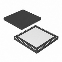
PIC24FJ256GA106-I/MR Microchip Technology, PIC24FJ256GA106-I/MR Datasheet - Page 2

PIC24FJ256GA106-I/MR
Manufacturer Part Number
PIC24FJ256GA106-I/MR
Description
IC, 16BIT MCU, PIC24F, 32MHZ, QFN-64
Manufacturer
Microchip Technology
Series
PIC® 24Fr
Datasheets
1.PIC24FJ128GA008-IPT.pdf
(12 pages)
2.PIC24FJ128GA106-IPT.pdf
(14 pages)
3.PIC24FJ128GA106-IPT.pdf
(330 pages)
4.PIC24FJ128GA106-IPT.pdf
(52 pages)
5.PIC24FJ256GA106-IPT.pdf
(59 pages)
6.PIC24FJ128GB110-IPF.pdf
(292 pages)
Specifications of PIC24FJ256GA106-I/MR
Controller Family/series
PIC24
No. Of I/o's
53
Ram Memory Size
16KB
Cpu Speed
32MHz
No. Of Timers
5
Core Size
16 Bit
Program Memory Size
256KB
Peripherals
ADC, Comparator, PWM, RTC, Timer
Core Processor
PIC
Speed
32MHz
Connectivity
I²C, PMP, SPI, UART/USART
Number Of I /o
53
Program Memory Type
FLASH
Ram Size
16K x 8
Voltage - Supply (vcc/vdd)
2 V ~ 3.6 V
Data Converters
A/D 16x10b
Oscillator Type
Internal
Operating Temperature
-40°C ~ 85°C
Package / Case
64-VFQFN, Exposed Pad
Processor Series
PIC24FJ
Core
PIC
Data Bus Width
16 bit
Data Ram Size
16 KB
Interface Type
I2C, SPI, UART
Maximum Clock Frequency
32 MHz
Number Of Programmable I/os
52
Number Of Timers
5
Maximum Operating Temperature
+ 85 C
Mounting Style
SMD/SMT
3rd Party Development Tools
52713-733, 52714-737, 53276-922, EWDSPIC
Development Tools By Supplier
PG164130, DV164035, DV244005, DV164005, PG164120, DM240001, DM240011
Minimum Operating Temperature
- 40 C
On-chip Adc
10 bit, 16 Channel
Lead Free Status / RoHS Status
Lead free / RoHS Compliant
For Use With
876-1004 - PIC24 BREAKOUT BOARD
Eeprom Size
-
Lead Free Status / Rohs Status
Details
regulator. The specifications for core voltage and capac-
PIC24FJXXXDA1/DA2/GB2/GA3
The
(Enhanced ICSP) protocol uses a faster method that
takes advantage of the programming executive, as
illustrated in
provides all the necessary functionality to erase, pro-
gram and verify the chip through a small command set.
The command set allows the programmer to program
the PIC24FJXXXDA1/DA2/GB2/GA3 MCUs without
having to deal with the low-level programming
protocols of the chip.
FIGURE 2-1:
This specification is divided into major sections that
describe the programming methods independently.
Section 3.0 “Device Programming – ICSP”
the In-Circuit Serial Programming method.
“Device Programming – Enhanced ICSP”
the Run-Time Self-Programming (RTSP) method.
2.1
All PIC24FJXXXDA1/DA2/GB2/GA3 devices power
their core digital logic at a nominal 1.8V. To simplify sys-
tem design, all devices in the PIC24FJXXXDA1/DA2/
GB2/GA3 families incorporate an on-chip regulator that
allows the device to run its core logic from V
PIC24F128GA310 family, the regulator is always
enabled, so there is no ENVREG pin on the device.
The regulator provides power to the core from the other
V
talum) must be connected to the V
and
itance are listed in
and Timing
DS39970B-page 2
DD
Programmer
Figure
pins. A low-ESR capacitor (such as ceramic or tan-
Enhanced
Power Requirements
2-2). This helps to maintain the stability of the
Requirements”.
Figure
Section 7.0 “AC/DC Characteristics
In-Circuit
2-1. The programming executive
PROGRAMMING SYSTEM
OVERVIEW FOR
ENHANCED ICSP™
PIC24FJXXXDA1/DA2/GB2/GA3
Serial
On-Chip Memory
CAP
Programming
Executive
pin (see
Programming
Section 4.0
DD
describes
describes
Table 2-1
. For the
operation. Any given word in memory must not be
written more than twice before erasing the page where it
2.2
The Flash program memory on PIC24FJXXXDA1/DA2/
GB2/GA3 devices has a specific write/erase require-
ment that must be adhered to for proper device
is located. Thus, the easiest way to conform to this rule
is to write all of the data in a programming block within
one write cycle. The programming methods specified in
this specification comply with this requirement.
2.3
Figure 2-4
for the PIC24FJXXXDA1/DA2/GB2/GA3 families. The
pins that are required for programming are listed in
Table 2-1
Refer to the appropriate device data sheet for complete
pin descriptions.
2.3.1
All of the devices in the PIC24FJXXXDA1/DA2/GB2/
GA3 families have three separate pairs of program-
ming pins, labelled as PGEC1/PGED1, PGEC2/PGED2
and PGEC3/PGED3. Any one of these pin pairs may be
used for device programming by either ICSP or
Enhanced ICSP. Unlike voltage supply and ground
pins, it is not necessary to connect all three pin pairs to
program the device. However, the programming
method must use both pins of the same pair.
FIGURE 2-2:
FIGURE 2-3:
Note:
Regulator Enabled (ENVREG tied to V
(10
Regulator Enabled (V
(10
C
C
EFC
EFC
F typ)
F typ)
Program Memory Write/Erase
Requirements
Pin Diagrams
and are indicated in bold text in the figures.
through
Writing to a location multiple times without
erasing is not recommended.
PGECx AND PGEDx PIN PAIRS
3.3V
3.3V
Figure 2-10
V
ENVREG
V
V
V
V
V
V
PIC24FJXXXDA1/DA2/GB2
PIC24FJXXXGA3
CONNECTIONS FOR THE
ON-CHIP REGULATOR
CONNECTIONS FOR THE
V
DD
CAP
SS
DD
BAT
CAP
SS
BAT
2010 Microchip Technology Inc.
BAT
tied to V
PIN
provide the pin diagrams
DD
or a Battery):
DD
):


