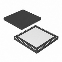
PIC24FJ256GA106-I/MR Microchip Technology, PIC24FJ256GA106-I/MR Datasheet - Page 3

PIC24FJ256GA106-I/MR
Manufacturer Part Number
PIC24FJ256GA106-I/MR
Description
IC, 16BIT MCU, PIC24F, 32MHZ, QFN-64
Manufacturer
Microchip Technology
Series
PIC® 24Fr
Datasheets
1.PIC24FJ128GA008-IPT.pdf
(12 pages)
2.PIC24FJ128GA106-IPT.pdf
(14 pages)
3.PIC24FJ128GA106-IPT.pdf
(330 pages)
4.PIC24FJ128GA106-IPT.pdf
(52 pages)
5.PIC24FJ256GA106-IPT.pdf
(59 pages)
6.PIC24FJ128GB110-IPF.pdf
(292 pages)
Specifications of PIC24FJ256GA106-I/MR
Controller Family/series
PIC24
No. Of I/o's
53
Ram Memory Size
16KB
Cpu Speed
32MHz
No. Of Timers
5
Core Size
16 Bit
Program Memory Size
256KB
Peripherals
ADC, Comparator, PWM, RTC, Timer
Core Processor
PIC
Speed
32MHz
Connectivity
I²C, PMP, SPI, UART/USART
Number Of I /o
53
Program Memory Type
FLASH
Ram Size
16K x 8
Voltage - Supply (vcc/vdd)
2 V ~ 3.6 V
Data Converters
A/D 16x10b
Oscillator Type
Internal
Operating Temperature
-40°C ~ 85°C
Package / Case
64-VFQFN, Exposed Pad
Processor Series
PIC24FJ
Core
PIC
Data Bus Width
16 bit
Data Ram Size
16 KB
Interface Type
I2C, SPI, UART
Maximum Clock Frequency
32 MHz
Number Of Programmable I/os
52
Number Of Timers
5
Maximum Operating Temperature
+ 85 C
Mounting Style
SMD/SMT
3rd Party Development Tools
52713-733, 52714-737, 53276-922, EWDSPIC
Development Tools By Supplier
PG164130, DV164035, DV244005, DV164005, PG164120, DM240001, DM240011
Minimum Operating Temperature
- 40 C
On-chip Adc
10 bit, 16 Channel
Lead Free Status / RoHS Status
Lead free / RoHS Compliant
For Use With
876-1004 - PIC24 BREAKOUT BOARD
Eeprom Size
-
Lead Free Status / Rohs Status
Details
TABLE 2-1:
FIGURE 2-4:
2010 Microchip Technology Inc.
Legend: I = Input, O = Output, P = Power
Note 1:
V
V
DD
SS
ENVREG
Pin Name
and AV
and AV
PGECx
PGEDx
MCLR
2:
V
CAP
All power supply and ground pins must be connected, including analog supplies (AV
(AV
There is no ENVREG pin in the GA310 family. The regulator is always enabled and the ENVREG pin is
replaced by the V
programming.
PGED3/AN4/C1INB/USBOEN/RP28/CN6/RB4
DD
SS
(2)
PGEC3/AN5/C1INA/V
SS
(1)
(1)
).
PIN DESCRIPTIONS (DURING PROGRAMMING)
ENVREG
PIN DIAGRAM (64-PIN TQFP)
PGED1/AN0/V
PGEC1/AN1/RP1/V
Pin Name
PGECx
PGED
MCLR
V
V
V
CAP
DD
SS
BAT
X
BUSON
(2)
pin. It is recommended to connect the V
REF
PIC24FJXXXDA1/DA2/GB2/GA3
/RP18/CN7/RB5
+/RP0/
Pin Type
REF
I/O
-/CN3/RB1
P
P
P
P
I
I
CN2/RB0
MCLR
RG6
RG7
RG8
RG9
RE5
RE6
RE7
RB3
RB2
V
V
DD
SS
Programming Enable
Enable for On-Chip Voltage Regulator
Power Supply
Ground
On-Chip Voltage Regulator Output to the Core
Programming Pin Pairs 1, 2 and 3: Serial Data
Programming Pin Pairs 1, 2 and 3: Serial Clock
10
11
12
13
14
15
16
1
2
3
4
5
6
7
8
9
During Programming
PIC24FJXXXDAX06
BAT
Pin Description
pin to the battery or V
48
47
46
45
44
43
42
41
40
39
38
37
36
35
34
33
DD
) and ground
DD
RC14
RC13
RD0
RD11
RD10
RD9
RD8
V
RC15
RC12
V
RG2
RG3
RF6
RF2
RF3
DS39970B-page 3
SS
DD
during


