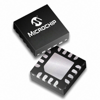
PIC16F610-E/ML Microchip Technology, PIC16F610-E/ML Datasheet - Page 120

PIC16F610-E/ML
Manufacturer Part Number
PIC16F610-E/ML
Description
1.75KB Flash, 64B RAM, 6 I/O, 8MHz Internal Oscillator 16 QFN 4x4mm TUBE
Manufacturer
Microchip Technology
Series
PIC® 16Fr
Datasheets
1.PIC12F609T-ISN.pdf
(26 pages)
2.PIC16F616T-ISL.pdf
(214 pages)
3.PIC16F616T-ISL.pdf
(8 pages)
Specifications of PIC16F610-E/ML
Core Processor
PIC
Core Size
8-Bit
Speed
20MHz
Peripherals
Brown-out Detect/Reset, POR, PWM, WDT
Number Of I /o
11
Program Memory Size
1.75KB (1K x 14)
Program Memory Type
FLASH
Ram Size
64 x 8
Voltage - Supply (vcc/vdd)
2 V ~ 5.5 V
Oscillator Type
Internal
Operating Temperature
-40°C ~ 125°C
Package / Case
16-QFN
Lead Free Status / RoHS Status
Lead free / RoHS Compliant
For Use With
AC162083 - HEADER MPLAB ICD2 PIC16F616 8/14AC164324 - MODULE SKT FOR MPLAB 8DFN/16QFNXLT16QFN1 - SOCKET TRANSITION 14DIP TO 16QFN
Eeprom Size
-
Data Converters
-
Connectivity
-
Lead Free Status / RoHS Status
Lead free / RoHS Compliant, Lead free / RoHS Compliant
- Current page: 120 of 214
- Download datasheet (4Mb)
PIC16F610/616/16HV610/616
FIGURE 12-8:
TABLE 12-6:
DS41288F-page 120
INTCON
IOCA
PIR1
PIE1
Legend:
Note
INSTRUCTION FLOW
GIE bit
(INTCON reg.)
INTF flag
(INTCON reg.)
Name
CLKOUT
INT pin
OSC1
Note 1: INTF flag is sampled here (every Q1).
Instruction
Executed
Instruction
Fetched
PC
1:
2: Asynchronous interrupt latency = 3-4 T
3: CLKOUT is available only in INTOSC and RC Oscillator modes.
4: For minimum width of INT pulse, refer to AC specifications in
5: INTF is enabled to be set any time during the Q4-Q1 cycles.
x = unknown, u = unchanged, – = unimplemented read as ‘0’, q = value depends upon condition.
Shaded cells are not used by the interrupt module.
PIC16F616/16HV616 only.
(3)
is the same whether Inst (PC) is a single cycle or a 2-cycle instruction.
Bit 7
GIE
—
—
—
SUMMARY OF REGISTERS ASSOCIATED WITH INTERRUPTS
Q1
Inst (PC – 1)
Inst (PC)
(1)
INT PIN INTERRUPT TIMING
ADIF
ADIE
Q2
PEIE
Bit 6
PC
—
(1)
(1)
(4)
Q3 Q4
CCP1IF
CCP1IE
IOCA5
(5)
Bit 5
T0IE
Q1
(1)
(1)
Inst (PC + 1)
Inst (PC)
IOCA4
Q2
(1)
Bit 4
INTE
C2IF
C2IE
PC + 1
Q3 Q4
CY
. Synchronous latency = 3 T
IOCA3
RAIE
Bit 3
C1IF
C1IE
Interrupt Latency
Q1
Dummy Cycle
IOCA2
Bit 2
T0IF
—
—
Q2
PC + 1
—
Q3 Q4
Section 15.0 “Electrical Specifications”
TMR2IE
TMR2IF
IOCA1
Bit 1
INTF
(2)
CY
(1)
(1)
, where T
Q1
Dummy Cycle
Inst (0004h)
TMR1IF
TMR1IE
Q2
IOCA0
RAIF
Bit 0
0004h
CY
= instruction cycle time. Latency
Q3 Q4
© 2009 Microchip Technology Inc.
0000 0000
--00 0000
-000 0-00
-000 0-00
POR, BOR
Value on
Q1
.
Inst (0005h)
Q2
Inst (0004h)
0005h
0000 0000
--00 0000
-000 0-00
-000 0-00
Q3 Q4
Value on
all other
Resets
Related parts for PIC16F610-E/ML
Image
Part Number
Description
Manufacturer
Datasheet
Request
R

Part Number:
Description:
IC PIC MCU FLASH 1KX14 14DIP
Manufacturer:
Microchip Technology
Datasheet:

Part Number:
Description:
IC PIC MCU FLASH 1KX14 16QFN
Manufacturer:
Microchip Technology
Datasheet:

Part Number:
Description:
IC PIC MCU FLASH 1KX14 14SOIC
Manufacturer:
Microchip Technology
Datasheet:

Part Number:
Description:
IC PIC MCU FLASH 1KX14 14TSSOP
Manufacturer:
Microchip Technology
Datasheet:

Part Number:
Description:
1.75KB Flash, 64B RAM, 6 I/O, 8MHz Internal Oscillator 14 PDIP .300in TUBE
Manufacturer:
Microchip Technology
Datasheet:

Part Number:
Description:
1.75KB Flash, 64B RAM, 6 I/O, 8MHz Internal Oscillator 14 SOIC .150in TUBE
Manufacturer:
Microchip Technology
Datasheet:

Part Number:
Description:
1.75KB Flash, 64B RAM, 6 I/O, 8MHz Internal Oscillator 14 TSSOP 4.4mm TUBE
Manufacturer:
Microchip Technology
Datasheet:

Part Number:
Description:
IC, 8BIT MCU, PIC16F, 32MHZ, SOIC-18
Manufacturer:
Microchip Technology
Datasheet:

Part Number:
Description:
IC, 8BIT MCU, PIC16F, 32MHZ, SSOP-20
Manufacturer:
Microchip Technology
Datasheet:

Part Number:
Description:
IC, 8BIT MCU, PIC16F, 32MHZ, DIP-18
Manufacturer:
Microchip Technology
Datasheet:

Part Number:
Description:
IC, 8BIT MCU, PIC16F, 32MHZ, QFN-28
Manufacturer:
Microchip Technology
Datasheet:

Part Number:
Description:
IC, 8BIT MCU, PIC16F, 32MHZ, QFN-28
Manufacturer:
Microchip Technology
Datasheet:

Part Number:
Description:
IC, 8BIT MCU, PIC16F, 32MHZ, QFN-28
Manufacturer:
Microchip Technology
Datasheet:

Part Number:
Description:
IC, 8BIT MCU, PIC16F, 32MHZ, SSOP-20
Manufacturer:
Microchip Technology
Datasheet:

Part Number:
Description:
IC, 8BIT MCU, PIC16F, 20MHZ, DIP-40
Manufacturer:
Microchip Technology
Datasheet:


