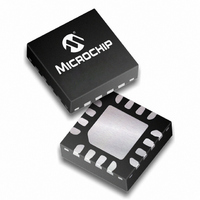
PIC16F610-E/ML Microchip Technology, PIC16F610-E/ML Datasheet - Page 90

PIC16F610-E/ML
Manufacturer Part Number
PIC16F610-E/ML
Description
1.75KB Flash, 64B RAM, 6 I/O, 8MHz Internal Oscillator 16 QFN 4x4mm TUBE
Manufacturer
Microchip Technology
Series
PIC® 16Fr
Datasheets
1.PIC12F609T-ISN.pdf
(26 pages)
2.PIC16F616T-ISL.pdf
(214 pages)
3.PIC16F616T-ISL.pdf
(8 pages)
Specifications of PIC16F610-E/ML
Core Processor
PIC
Core Size
8-Bit
Speed
20MHz
Peripherals
Brown-out Detect/Reset, POR, PWM, WDT
Number Of I /o
11
Program Memory Size
1.75KB (1K x 14)
Program Memory Type
FLASH
Ram Size
64 x 8
Voltage - Supply (vcc/vdd)
2 V ~ 5.5 V
Oscillator Type
Internal
Operating Temperature
-40°C ~ 125°C
Package / Case
16-QFN
Lead Free Status / RoHS Status
Lead free / RoHS Compliant
For Use With
AC162083 - HEADER MPLAB ICD2 PIC16F616 8/14AC164324 - MODULE SKT FOR MPLAB 8DFN/16QFNXLT16QFN1 - SOCKET TRANSITION 14DIP TO 16QFN
Eeprom Size
-
Data Converters
-
Connectivity
-
Lead Free Status / RoHS Status
Lead free / RoHS Compliant, Lead free / RoHS Compliant
- Current page: 90 of 214
- Download datasheet (4Mb)
PIC16F610/616/16HV610/616
10.3
The PWM mode generates a Pulse-Width Modulated
signal on the CCP1 pin. The duty cycle, period and
resolution are determined by the following registers:
• PR2
• T2CON
• CCPR1L
• CCP1CON
In Pulse-Width Modulation (PWM) mode, the CCP
module produces up to a 10-bit resolution PWM output
on the CCP1 pin. Since the CCP1 pin is multiplexed
with the PORT data latch, the TRIS for that pin must be
cleared to make the CCP1 pin an output.
Figure 10-3 shows a simplified block diagram of PWM
operation.
Figure 10-4 shows a typical waveform of the PWM
signal.
For a step-by-step procedure on how to set up the CCP
module for PWM operation, see Section 10.3.7
“Setup for PWM Operation”.
FIGURE 10-3:
DS41288F-page 90
Note 1:
Note:
CCPR1H
Duty Cycle Registers
Comparator
2:
CCPR1L
PWM Mode
PR2
TMR2
Comparator
Clearing the CCP1CON register will
relinquish CCP1 control of the CCP1 pin.
The 8-bit timer TMR2 register is concatenated
with the 2-bit internal system clock (F
2 bits of the prescaler, to create the 10-bit time
base.
In PWM mode, CCPR1H is a read-only register.
(2)
(Slave)
(1)
SIMPLIFIED PWM BLOCK
DIAGRAM
Clear Timer2,
toggle CCP1 pin and
latch duty cycle
CCP1CON<5:4>
S
R
Q
TRIS
OSC
CCP1
), or
The PWM output (Figure 10-4) has a time base
(period) and a time that the output stays high (duty
cycle).
FIGURE 10-4:
Pulse Width
TMR2 = 0
Period
CCP PWM OUTPUT
TMR2 = CCPR1L:CCP1CON<5:4>
© 2009 Microchip Technology Inc.
TMR2 = PR2
Related parts for PIC16F610-E/ML
Image
Part Number
Description
Manufacturer
Datasheet
Request
R

Part Number:
Description:
IC PIC MCU FLASH 1KX14 14DIP
Manufacturer:
Microchip Technology
Datasheet:

Part Number:
Description:
IC PIC MCU FLASH 1KX14 16QFN
Manufacturer:
Microchip Technology
Datasheet:

Part Number:
Description:
IC PIC MCU FLASH 1KX14 14SOIC
Manufacturer:
Microchip Technology
Datasheet:

Part Number:
Description:
IC PIC MCU FLASH 1KX14 14TSSOP
Manufacturer:
Microchip Technology
Datasheet:

Part Number:
Description:
1.75KB Flash, 64B RAM, 6 I/O, 8MHz Internal Oscillator 14 PDIP .300in TUBE
Manufacturer:
Microchip Technology
Datasheet:

Part Number:
Description:
1.75KB Flash, 64B RAM, 6 I/O, 8MHz Internal Oscillator 14 SOIC .150in TUBE
Manufacturer:
Microchip Technology
Datasheet:

Part Number:
Description:
1.75KB Flash, 64B RAM, 6 I/O, 8MHz Internal Oscillator 14 TSSOP 4.4mm TUBE
Manufacturer:
Microchip Technology
Datasheet:

Part Number:
Description:
IC, 8BIT MCU, PIC16F, 32MHZ, SOIC-18
Manufacturer:
Microchip Technology
Datasheet:

Part Number:
Description:
IC, 8BIT MCU, PIC16F, 32MHZ, SSOP-20
Manufacturer:
Microchip Technology
Datasheet:

Part Number:
Description:
IC, 8BIT MCU, PIC16F, 32MHZ, DIP-18
Manufacturer:
Microchip Technology
Datasheet:

Part Number:
Description:
IC, 8BIT MCU, PIC16F, 32MHZ, QFN-28
Manufacturer:
Microchip Technology
Datasheet:

Part Number:
Description:
IC, 8BIT MCU, PIC16F, 32MHZ, QFN-28
Manufacturer:
Microchip Technology
Datasheet:

Part Number:
Description:
IC, 8BIT MCU, PIC16F, 32MHZ, QFN-28
Manufacturer:
Microchip Technology
Datasheet:

Part Number:
Description:
IC, 8BIT MCU, PIC16F, 32MHZ, SSOP-20
Manufacturer:
Microchip Technology
Datasheet:

Part Number:
Description:
IC, 8BIT MCU, PIC16F, 20MHZ, DIP-40
Manufacturer:
Microchip Technology
Datasheet:


