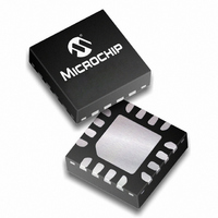
PIC16F610-E/ML Microchip Technology, PIC16F610-E/ML Datasheet - Page 126

PIC16F610-E/ML
Manufacturer Part Number
PIC16F610-E/ML
Description
1.75KB Flash, 64B RAM, 6 I/O, 8MHz Internal Oscillator 16 QFN 4x4mm TUBE
Manufacturer
Microchip Technology
Series
PIC® 16Fr
Datasheets
1.PIC12F609T-ISN.pdf
(26 pages)
2.PIC16F616T-ISL.pdf
(214 pages)
3.PIC16F616T-ISL.pdf
(8 pages)
Specifications of PIC16F610-E/ML
Core Processor
PIC
Core Size
8-Bit
Speed
20MHz
Peripherals
Brown-out Detect/Reset, POR, PWM, WDT
Number Of I /o
11
Program Memory Size
1.75KB (1K x 14)
Program Memory Type
FLASH
Ram Size
64 x 8
Voltage - Supply (vcc/vdd)
2 V ~ 5.5 V
Oscillator Type
Internal
Operating Temperature
-40°C ~ 125°C
Package / Case
16-QFN
Lead Free Status / RoHS Status
Lead free / RoHS Compliant
For Use With
AC162083 - HEADER MPLAB ICD2 PIC16F616 8/14AC164324 - MODULE SKT FOR MPLAB 8DFN/16QFNXLT16QFN1 - SOCKET TRANSITION 14DIP TO 16QFN
Eeprom Size
-
Data Converters
-
Connectivity
-
Lead Free Status / RoHS Status
Lead free / RoHS Compliant, Lead free / RoHS Compliant
- Current page: 126 of 214
- Download datasheet (4Mb)
PIC16F610/616/16HV610/616
12.10 In-Circuit Serial Programming™
The PIC16F610/616/16HV610/616 microcontrollers
can be serially programmed while in the end
application circuit. This is simply done with five
connections for:
• clock
• data
• power
• ground
• programming voltage
This allows customers to manufacture boards with
unprogrammed devices and then program the
microcontroller just before shipping the product. This
also allows the most recent firmware or a custom
firmware to be programmed.
The device is placed into a Program/Verify mode by
holding the RA0 and RA1 pins low, while raising the
MCLR (V
Programming Specification (DS41284) for more
information. RA0 becomes the programming data and
RA1 becomes the programming clock. Both RA0 and
RA1 are Schmitt Trigger inputs in Program/Verify
mode.
A typical In-Circuit Serial Programming connection is
shown in Figure 12-10.
FIGURE 12-10:
DS41288F-page 126
External
Connector
Signals
* Isolation devices (as required)
Data I/O
CLK
+5V
V
0V
PP
PP
) pin from V
*
To Normal
Connections
To Normal
Connections
TYPICAL IN-CIRCUIT
SERIAL
PROGRAMMING™
CONNECTION
*
IL
*
to V
*
IHH
V
V
MCLR/V
GP1
GP0
PIC12F615/12HV615
PIC12F609/12HV609
DD
SS
. See the Memory
PP
/GP3/RA3
12.11 In-Circuit Debugger
Since in-circuit debugging requires access to three pins,
MPLAB
not practical. A special 28-pin PIC16F610/616/
16HV610/616 ICD device is used with MPLAB ICD 2 to
provide separate clock, data and MCLR pins and frees
all normally available pins to the user.
A special debugging adapter allows the ICD device to
be used in place of a PIC16F610/616/16HV610/616
device. The debugging adapter is the only source of the
ICD device.
When the ICD pin on the PIC16F610/616/16HV610/
616 ICD device is held low, the In-Circuit Debugger
functionality is enabled. This function allows simple
debugging functions when used with MPLAB ICD 2.
When the microcontroller has this feature enabled,
some of the resources are not available for general
use. Table 12-9 shows which features are consumed
by the background debugger.
TABLE 12-9:
For more information, see “MPLAB
Debugger User’s Guide” (DS51331), available on
Microchip’s web site (www.microchip.com).
Resource
I/O pins
Stack
Program Memory
Note:
®
ICD 2 development with an 14-pin device is
To erase the device V
the Bulk Erase V
Memory
(DS41284)
DEBUGGER RESOURCES
Description
ICDCLK, ICDDATA
1 level
Address 0h must be NOP
700h-7FFh
Programming
© 2009 Microchip Technology Inc.
DD
minimum given in the
DD
®
must be above
ICD 2 In-Circuit
Specification
Related parts for PIC16F610-E/ML
Image
Part Number
Description
Manufacturer
Datasheet
Request
R

Part Number:
Description:
IC PIC MCU FLASH 1KX14 14DIP
Manufacturer:
Microchip Technology
Datasheet:

Part Number:
Description:
IC PIC MCU FLASH 1KX14 16QFN
Manufacturer:
Microchip Technology
Datasheet:

Part Number:
Description:
IC PIC MCU FLASH 1KX14 14SOIC
Manufacturer:
Microchip Technology
Datasheet:

Part Number:
Description:
IC PIC MCU FLASH 1KX14 14TSSOP
Manufacturer:
Microchip Technology
Datasheet:

Part Number:
Description:
1.75KB Flash, 64B RAM, 6 I/O, 8MHz Internal Oscillator 14 PDIP .300in TUBE
Manufacturer:
Microchip Technology
Datasheet:

Part Number:
Description:
1.75KB Flash, 64B RAM, 6 I/O, 8MHz Internal Oscillator 14 SOIC .150in TUBE
Manufacturer:
Microchip Technology
Datasheet:

Part Number:
Description:
1.75KB Flash, 64B RAM, 6 I/O, 8MHz Internal Oscillator 14 TSSOP 4.4mm TUBE
Manufacturer:
Microchip Technology
Datasheet:

Part Number:
Description:
IC, 8BIT MCU, PIC16F, 32MHZ, SOIC-18
Manufacturer:
Microchip Technology
Datasheet:

Part Number:
Description:
IC, 8BIT MCU, PIC16F, 32MHZ, SSOP-20
Manufacturer:
Microchip Technology
Datasheet:

Part Number:
Description:
IC, 8BIT MCU, PIC16F, 32MHZ, DIP-18
Manufacturer:
Microchip Technology
Datasheet:

Part Number:
Description:
IC, 8BIT MCU, PIC16F, 32MHZ, QFN-28
Manufacturer:
Microchip Technology
Datasheet:

Part Number:
Description:
IC, 8BIT MCU, PIC16F, 32MHZ, QFN-28
Manufacturer:
Microchip Technology
Datasheet:

Part Number:
Description:
IC, 8BIT MCU, PIC16F, 32MHZ, QFN-28
Manufacturer:
Microchip Technology
Datasheet:

Part Number:
Description:
IC, 8BIT MCU, PIC16F, 32MHZ, SSOP-20
Manufacturer:
Microchip Technology
Datasheet:

Part Number:
Description:
IC, 8BIT MCU, PIC16F, 20MHZ, DIP-40
Manufacturer:
Microchip Technology
Datasheet:


