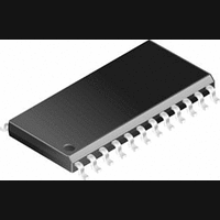
USBN9604-28M National Semiconductor, USBN9604-28M Datasheet - Page 10

USBN9604-28M
Manufacturer Part Number
USBN9604-28M
Description
Special Function IC
Manufacturer
National Semiconductor
Datasheet
1.USBN9604-28M.pdf
(60 pages)
Specifications of USBN9604-28M
Peak Reflow Compatible (260 C)
No
Leaded Process Compatible
No
Mounting Type
Surface Mount
Package / Case
28-WSOIC
Lead Free Status / RoHS Status
Contains lead / RoHS non-compliant
Available stocks
Company
Part Number
Manufacturer
Quantity
Price
Part Number:
USBN9604-28M
Manufacturer:
NS/国半
Quantity:
20 000
Company:
Part Number:
USBN9604-28M/NOPB
Manufacturer:
Freescale
Quantity:
2 314
Part Number:
USBN9604-28M/NOPB
Manufacturer:
TI/德州仪器
Quantity:
20 000
Part Number:
USBN9604-28MX
Manufacturer:
NS/国半
Quantity:
20 000
Company:
Part Number:
USBN9604-28MX/NOPB
Manufacturer:
NS21
Quantity:
1 495
Part Number:
USBN9604-28MX/NOPB
Manufacturer:
TI/德州仪器
Quantity:
20 000
www.national.com
2.0 Functional Overview
The device is a Universal Serial Bus (USB) Node controller compatible with USB Specification, 1.0 and 1.1. It integrates onto
a single IC the required USB transceiver with a 3.3V regulator, the Serial Interface Engine (SIE), USB endpoint FIFOs, a
versatile (8-bit parallel or serial) interface and a clock generator. A total of seven endpoint pipes are supported: one bidirec-
tional for the mandatory control EP0 and an additional six for unidirectional endpoints to support USB interrupt, bulk and
isochronous data transfers. The 8-bit parallel interface supports multiplexed and non-multiplexed style CPU address/data
buses. The synchronous serial MICROWIRE interface allows adapting to CPUs without external address/data buses. A pro-
grammable interrupt output scheme allows adapting to different interrupt signaling requirements.
Refer to Figure 2 for the major functional blocks, described in the following sections.
2.1 TRANSCEIVER
The device contains a high-speed transceiver which consists of three main functional blocks:
This transceiver meets the performance requirements described in Chapter 7 of the USB Specification, Version 1.1.
To minimize signal skew, the differential output swings of the transmitter are well balanced. Slew-rate control is used on the
driver to minimize radiated noise and crosstalk. The drivers support TRI-STATE operation to allow bidirectional, half-duplex
operation of the transceiver.
The differential receiver operates over the complete common mode range, and has a delay guaranteed to be larger than
that of the single-ended receivers. This avoids potential glitches in the Serial Interface Engine (SIE) after single-ended ze-
ros.
Single-ended receivers are present on each of the two data lines. These are required, in addition to the differential receiver, to
detect an absolute voltage with a switching threshold between 0.8V and 2.0V (TTL inputs). To increase V
glitching, a voltage reference sets the single-ended switching reference. An external 1.5 5% K resistor is required on D+ to
indicate that this is a high-speed node. This resistor should be tied to a voltage source between 3.0V and 3.6V, and referenced
to the local ground, such as the output provided on pin V3.3.
2.2 VOLTAGE REGULATOR (VREG)
The voltage regulator provides 3.3V for the integrated transceiver from 5.0V device power or USB bus power. This output
can be used to supply power to the 1.5 K pull-up resistor. This output must be decoupled with a 1 F tantalum capacitor
to ground. It can be disabled under software control to allow using the device in a 3.3V system.
2.3 SERIAL INTERFACE ENGINE (SIE)
The SIE is comprised of physical (PHY) and Media Access Controller (MAC) modules. The PHY module includes the digital-
clock recovery circuit, a digital glitch filter, End Of Packet (EOP) detection circuitry, and bit stuffing and unstuffing logic. The
MAC module includes packet formatting, CRC generation and checking, and endpoint address detection. It provides the
necessary control to give the NAK, ACK and STALL responses as determined by the Endpoint Pipe Controller (EPC) for the
specified endpoint pipe. The SIE is also responsible for detecting and reporting USB-specific events, such as NodeReset,
NodeSuspend and NodeResume. The module output signals to the transceiver are well matched (under 1 nS) to minimize
skew on the USB signals.
The USB specifications assign bit stuffing and unstuffing as the method to ensure adequate electrical transitions on the line
to enable clock recovery at the receiving end. The bit stuffing block ensures that whenever a string of consecutive 1’s is
encountered, a 0 is inserted after every sixth 1 in the data stream. The bit unstuffing logic reverses this process.
The clock recovery block uses the incoming NRZI data to extract a data clock (12 MHz) from a 48 MHz input clock. This
input clock is derived from a 24 MHz oscillator in conjunction with PLL circuitry (clock doubler). This clock is used in the data
recovery circuit. The output of this block is binary data (decoded from the NRZI stream) which can be appropriately sampled
using the extracted 12 MHz clock. The jitter performance and timing characteristics meet the requirements set forth in Chap-
ter 7 of the USB Specification.
— Differential receiver
— Single-ended receiver with on-chip voltage reference
— Transmitter with on-chip current source.
10
cc
rejection, without


