IXTH30N60L2 IXYS SEMICONDUCTOR, IXTH30N60L2 Datasheet
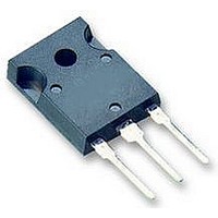
MOSFET,N CH,600V,30A,TO-247

IXTH30N60L2

Manufacturer Part Number
IXTH30N60L2
Description
MOSFET,N CH,600V,30A,TO-247
Manufacturer
IXYS SEMICONDUCTOR
Datasheet

Specifications of IXTH30N60L2

Transistor Polarity
N Channel
Drain Source Voltage Vds
600V
On Resistance Rds(on)
240mohm
Rds(on) Test Voltage Vgs
10V
Voltage Vgs Max
20V
Operating Temperature Range
-55°C To +150°C
Transistor Case
RoHS Compliant
Transistor Case Style
TO-247
Rohs Compliant
Yes
Linear L2
MOSFET with extended
FBSOA
N-Channel Enhancement Mode
Avalanche rated
Symbol
V
V
V
V
I
I
I
E
P
T
T
T
T
T
M
Weight
Symbol
(T
BV
V
I
I
R
© 2009 IXYS CORPORATION, All rights reserved
D25
DM
A
GSS
DSS
J
JM
stg
L
SOLD
DSS
DGR
GSS
GSM
AS
D
GS(th)
DS(on)
d
J
DSS
= 25°C, unless otherwise specified)
T
T
Continuous
Transient
T
T
T
T
T
1.6mm (0.063in) from case for 10s
Plastic body for 10s
Mounting torque (TO-247&TO-3P)
TO-247
TO-3P
TO-268
V
V
V
V
V
V
Test Conditions
Test Conditions
J
J
C
C
C
C
C
GS
DS
GS
DS
GS
GS
TM
= 25°C to 150°C
= 25°C to 150°C, R
= 25°C
= 25°C, pulse width limited by T
= 25°C
= 25°C
= 25°C
= 10V, I
= 0V, I
= V
= ±20V, V
= V
= 0V
GS
DSS
Power
, I
D
D
D
= 1mA
= 250μA
= 0.5 • I
DS
= 0V
D25
GS
, Note 1
= 1MΩ
Preliminary Technical Information
T
J
= 125°C
JM
IXTH30N60L2
IXTQ30N60L2
IXTT30N60L2
-55 to +150
-55 to +150
Characteristic Values
Min.
600
2.5
1.13/10
Maximum Ratings
+150
±30
540
300
260
600
600
±20
6.0
4.0
5.5
80
30
30
2
Typ.
±100
300
240 mΩ
Nm/lb.in.
Max.
4.5
50
μA
μA
°C
nA
°C
°C
°C
°C
W
V
V
V
V
A
A
A
V
V
g
g
g
J
V
I
R
TO-247
TO-3P
TO-268
G = Gate
S = Source
Features
Applications
D25
Designed for linear operation
International standard packages
Avalanche rated
Molding epoxies meet UL 94 V-0
flammability classification
Guaranteed FBSOA at 75°C
Solid state circuit breakers
Soft start controls
Linear amplifiers
Programmable loads
Current regulators
DS(on)
DSS
G
D
S
G
≤ ≤ ≤ ≤ ≤ 240mΩ Ω Ω Ω Ω
= 600V
= 30A
S
TAB = Drain
D
= Drain
DS100101(01/09)
(TAB)
(TAB)
(TAB)

Related parts for IXTH30N60L2

IXTH30N60L2 Summary of contents

Page 1

... GSS DSS DS DSS 0.5 • 10V, I DS(on D25 © 2009 IXYS CORPORATION, All rights reserved Preliminary Technical Information IXTH30N60L2 IXTQ30N60L2 IXTT30N60L2 Maximum Ratings 600 = 1MΩ 600 GS ±20 ± 540 -55 to +150 +150 -55 to +150 300 260 1.13/10 6.0 5.5 4.0 Characteristic Values Min ...

Page 2

... C Characteristic Values (T = 25°C, unless otherwise specified) J Min. Typ 100V 710 R 4,931,844 5,049,961 5,237,481 6,162,665 5,017,508 5,063,307 5,381,025 6,259,123 B1 5,034,796 5,187,117 5,486,715 6,306,728 B1 IXTH30N60L2 IXTQ30N60L2 IXTT30N60L2 TO-247 (IXTH) Outline Max Terminals Gate Source Dim. Millimeter nC Min. Max 4 ...

Page 3

... D © 2009 IXYS CORPORATION, All rights reserved 14V 12V 10V 20V 12V 10V 15A Value 125º 25º IXTH30N60L2 IXTQ30N60L2 Fig. 2. Extended Output Characteristics @ 25º 20V GS 14V 70 12V 10V Volts DS Fig Normalized to I DS(on) vs. Junction Temperature 2.8 2 10V GS 2.4 2.2 2.0 1 ...

Page 4

... IXYS reserves the right to change limits, test conditions, and dimensions 125ºC J 25ºC - 40ºC 6.5 7.0 7.5 8.0 8.5 9 25ºC J 0.7 0.8 0.9 1.0 1.000 C iss 0.100 C oss 0.010 C rss 0.001 IXTH30N60L2 IXTQ30N60L2 Fig. 8. Transconductance Amperes D Fig. 10. Gate Charge 16 V ...

Page 5

... C Single Pulse 0.1 10 100 V - Volts DS © 2009 IXYS CORPORATION, All rights reserved = 25ºC 100.0 25µs 100µs 10.0 1ms 10ms 100ms DC 1000 IXTH30N60L2 IXTQ30N60L2 Fig. 14. Forward-Bias Safe Operating Area @ T = 75º Limit DS(on) 1 150º 75ºC C Single Pulse 0.1 10 100 V ...

Related keywords