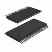
74CBTLV16211DGV NXP Semiconductors, 74CBTLV16211DGV Datasheet - Page 4

74CBTLV16211DGV
Manufacturer Part Number
74CBTLV16211DGV
Description
74CBTLV16211DGV/TSSOP56/REEL13
Manufacturer
NXP Semiconductors
Datasheet
1.74CBTLV16211DGG11.pdf
(16 pages)
Specifications of 74CBTLV16211DGV
Number Of Switches
Dual
Propagation Delay Time
0.2 ns
Supply Voltage (max)
3.6 V
Supply Voltage (min)
2.3 V
Maximum Operating Temperature
+ 125 C
Minimum Operating Temperature
- 40 C
Package / Case
TSOP-56
Maximum Power Dissipation
600 mW
Mounting Style
SMD/SMT
Off Time (max)
8.8 ns
On Resistance (max)
60 Ohms
On Time (max)
7.8 ns
Supply Current
100 mA
Switch Current (typ)
100 mA
Lead Free Status / RoHS Status
Lead free / RoHS Compliant
Lead Free Status / RoHS Status
Lead free / RoHS Compliant
Other names
568-5260-2
Available stocks
Company
Part Number
Manufacturer
Quantity
Price
NXP Semiconductors
Table 2.
6. Functional description
Table 3.
[1]
7. Limiting values
Table 4.
In accordance with the Absolute Maximum Rating System (IEC 60134). Voltages are referenced to GND (ground = 0 V).
[1]
[2]
8. Recommended operating conditions
Table 5.
[1]
74CBTLV16211
Product data sheet
Symbol
1B0 to 1B11
2OE
1OE
Output enable input OE
L
H
Symbol
V
V
V
I
I
I
I
I
T
P
Symbol
V
V
V
T
t/V
IK
SK
SW
CC
GND
stg
amb
CC
I
SW
tot
CC
I
SW
H = HIGH voltage level; L = LOW voltage level.
The minimum input and output voltage ratings may be exceeded if the input and output current ratings are observed.
For TSSOP56 packages: above 55 C the value of P
Applies to control signal levels.
Pin description
Function table
Limiting values
Recommended operating conditions
Parameter
supply voltage
input voltage
switch voltage
input clamping current
switch clamping current
switch current
supply current
ground current
storage temperature
total power dissipation
Parameter
supply voltage
input voltage
switch voltage
ambient temperature
input transition rise and fall rate
Pin
54, 53, 52, 51, 50, 48, 47, 46, 45, 44, 43, 42
55
56
[1]
…continued
All information provided in this document is subject to legal disclaimers.
Conditions
enable and disable mode
V
V
V
T
amb
I
I
SW
< 0.5 V
< 0.5 V
= 0 V to V
= 40 C to +125 C
Rev. 5 — 30 December 2010
Conditions
enable and disable mode
V
CC
tot
derates linearly with 8.0 mW/K.
= 2.3 V to 3.6 V
CC
Function switch
ON-state
OFF-state
independent input or output
Description
output enable input (active-LOW)
output enable input (active-LOW)
[1]
[1]
[2]
Min
0.5
0.5
0.5
50
50
-
-
100
65
-
74CBTLV16211
[1]
Min
2.3
0
0
40
0
Max
+4.6
+4.6
V
-
-
128
+100
-
+150
600
CC
© NXP B.V. 2010. All rights reserved.
24-bit bus switch
+ 0.5
Max
3.6
3.6
V
+125
200
CC
Unit
V
V
V
mA
mA
mA
mA
mA
C
mW
Unit
V
V
V
C
ns/V
4 of 16


