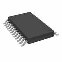
AD8188ARUZ Analog Devices Inc, AD8188ARUZ Datasheet - Page 15

AD8188ARUZ
Manufacturer Part Number
AD8188ARUZ
Description
IC,ANALOG MUX,TRIPLE,2-CHANNEL,TSSOP,24PIN,PLASTIC
Manufacturer
Analog Devices Inc
Type
Analog Multiplexerr
Datasheet
1.AD8188ARUZ.pdf
(24 pages)
Specifications of AD8188ARUZ
Function
Multiplexer
Circuit
3 x 2:1
On-state Resistance
350 mOhm
Voltage Supply Source
Single Supply
Voltage - Supply, Single/dual (±)
3.5 V ~ 5.5 V
Current - Supply
15mA
Operating Temperature
-40°C ~ 85°C
Mounting Type
Surface Mount
Package / Case
24-TSSOP (0.173", 4.40mm Width)
Package
24TSSOP
Multiplexer Architecture
2:1
Maximum Turn-off Time
17(Typ)@5V ns
Maximum Turn-on Time
4(Typ)@5V ns
Power Supply Type
Single
Lead Free Status / RoHS Status
Lead free / RoHS Compliant
Available stocks
Company
Part Number
Manufacturer
Quantity
Price
Company:
Part Number:
AD8188ARUZ
Manufacturer:
NVE
Quantity:
35
Part Number:
AD8188ARUZ
Manufacturer:
ADI/亚德诺
Quantity:
20 000
The AD8189
The AD8189 uses on-chip feedback resistors to realize the gain-
of-two function. To provide low crosstalk and a high output
impedance when disabled, each set of 500 Ω feedback resistors
is terminated by a dedicated reference buffer. A reference buffer
is a high speed op amp configured as a unity-gain follower. The
three reference buffers, one for each channel, share a single,
high impedance input, the V
bias current is typically less than 2 μA.
This configuration has a few implications for single-supply
operation:
•
Figure 46. Conceptual Diagram of a Single Multiplexer Channel, G = 2
On the AD8189, V
analog supply, V
Figure 47):
V
1.3 V < V
Figure 45. V
EE
+ 1.3 V < V
DIRECT CONNECTION TO ANY “QUIET” AC GROUND
(FOR EXAMPLE, GND, V
V
V
REF
A0
B0
REF
IN0A
IN0B
IN1A
IN1B
IN2A
IN2B
REF
REF
, 3.4 V on 0 V/5 V supplies
Pin Connection for AD8188 (Differs from AD8189)
REF
EE
INTERNAL CAP
. The limits on reference voltage are (see
× V
REF
BIAS REFERENCE
5V
5V
5V
GBUF 0
5V
GBUF 1
5V
GBUF 2
cannot be tied to the most negative
“C_BYPASS”
CC
MUX SYSTEM
AD8188
REF
CC
− 1.6 V
500Ω
500Ω
, AND V
pin (see Figure 46). V
VF-1
VF-2
500Ω
500Ω
EE
1×
500Ω
500Ω
).
VFO
OUT0
OUT1
OUT2
OUT0
OUT1
OUT2
REF
input
Rev. 0 | Page 15 of 24
•
•
If system considerations prevent running the multiplexer on
split supplies, a false ground reference should be employed. A
low impedance reference can be synthesized with a second
operational amplifier. Alternately, a well bypassed resistor
divider can be used. Refer to the Applications section for
further explanation and more examples.
Figure 47. Output Compliance of Main Amplifier Channel and Ground Buffer
The signal at the V
Therefore, V
impedance source. Using superposition, it is shown that
V
To maximize the output dynamic range, the reference
voltage should be chosen with care. For example, consider
amplifying a 700 mV video signal with a sync pulse
300 mV below black level. If the user decides to set V
black level to preferentially run video signals on the faster
NPN transistor path, the AD8189 allows a reference
voltage as low as 1.3 V + 300 mV = 1.6 V. If the AD8189 is
used, the sync pulse is amplified to 600 mV. Therefore, the
lower limit on V
routing RGB video, an advantageous configuration is to
employ +3 V and −2 V supplies, in which case V
tied to ground.
V
OUT
REF
A0
= 2 × V
GND
5V
Figure 48. Synthesis of a False Ground Reference
100kΩ
5V
5V
REF
IN
1µF
FROM 1992 ADI AMPLIFIER
APPLICATIONS GUIDE
− V
should be tied to a well bypassed, low
REF
REF
REF
becomes 1.3 V + 600 mV = 1.9 V. For
pin appears at each output.
OP21
OUT0
1.3V
1.3V
1.6V
1.3V
0.022µF
10kΩ
100Ω
AD8188/AD8189
1µF
5V
5V
V
V
GND
V
V
GND
V
O_MAX
O_MIN
O_MAX
O_MIN
REF
V
V
REF
OUT
= 1.3V
= 1.3V
= 3.7V
= 3.4V
REF
can be
REF
at


