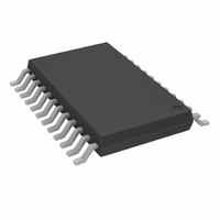
AD8188ARUZ Analog Devices Inc, AD8188ARUZ Datasheet - Page 16

AD8188ARUZ
Manufacturer Part Number
AD8188ARUZ
Description
IC,ANALOG MUX,TRIPLE,2-CHANNEL,TSSOP,24PIN,PLASTIC
Manufacturer
Analog Devices Inc
Type
Analog Multiplexerr
Datasheet
1.AD8188ARUZ.pdf
(24 pages)
Specifications of AD8188ARUZ
Function
Multiplexer
Circuit
3 x 2:1
On-state Resistance
350 mOhm
Voltage Supply Source
Single Supply
Voltage - Supply, Single/dual (±)
3.5 V ~ 5.5 V
Current - Supply
15mA
Operating Temperature
-40°C ~ 85°C
Mounting Type
Surface Mount
Package / Case
24-TSSOP (0.173", 4.40mm Width)
Package
24TSSOP
Multiplexer Architecture
2:1
Maximum Turn-off Time
17(Typ)@5V ns
Maximum Turn-on Time
4(Typ)@5V ns
Power Supply Type
Single
Lead Free Status / RoHS Status
Lead free / RoHS Compliant
Available stocks
Company
Part Number
Manufacturer
Quantity
Price
Company:
Part Number:
AD8188ARUZ
Manufacturer:
NVE
Quantity:
35
Part Number:
AD8188ARUZ
Manufacturer:
ADI/亚德诺
Quantity:
20 000
AD8188/AD8189
AC-COUPLED INPUTS
Using ac-coupled inputs presents an interesting challenge for
video systems operating from a single 5 V supply. In NTSC and
PAL video systems, 700 mV is the approximate difference
between the maximum signal voltage and black level. It is
assumed that sync has been stripped. However, given the two
pathological cases shown in Figure 50, a dynamic range of twice
the maximum signal swing is required if the inputs are to be
ac-coupled. A possible solution is to use a dc restore circuit
before the mux.
TOLERANCE TO CAPACITIVE LOAD
Op amps are sensitive to reactive loads. A capacitive load at the
output appears in parallel with an effective resistance (R
where R
output impedance, approximately 15 Ω for these muxes.
The load pole (f
can seriously degrade phase margin and, therefore, stability. The
old workaround is to place a small series resistor directly at the
output to isolate the load pole. While effective, this ruse also
affects the dc and termination characteristics of a 75 Ω system.
The AD8188 and AD8189 are built with a variable compensation
scheme that senses the output reactance and trades bandwidth
for phase margin, ensuring faster settling and lower overshoot
at higher capacitive loads.
Figure 49. Alternate Method for Synthesis of a False Ground Reference
R
BLACK LINE WITH WHITE PIXEL
f
V
EFF
LOAD
REF
+700mV
L
= ( R
Figure 50. Pathological Case for Input Dynamic Range
is the discrete resistive load, and r
=
L
2
|| r
π
V
LOAD
SIGNAL
R
O
EFF
)
1
10kΩ
10kΩ
CAP MUST BE LARGE
ENOUGH TO ABSORB
TRANSIENT CURRENTS
WITH MINIMUM BOUNCE.
) at
C
5V
L
GND
V
+5V
AVG
WHITE LINE WITH BLACK PIXEL
V
1µF
AVG
V
V
V
SET BY THE RESISTORS
INPUT
REF
REF
V
~ V
IS A DC VOLTAGE
REF
= V
AVG
REF
O
is the open loop
+ V
–700mV
SIGNAL
V
REF
EFF
) of
Rev. 0 | Page 16 of 24
SECONDARY SUPPLIES AND SUPPLY BYPASSING
The high current output transistors are given their own supply
pins (Pin 15, Pin 17, Pin 19, and Pin 21) to reduce supply noise
on-chip and to improve output isolation. Because these
secondary, high current supply pins are not connected on-chip
to the primary analog supplies, V
Pin 11, Pin 13, and Pin 24), some care should be taken to ensure
that the supply bypass capacitors are connected to the correct
pins. At a minimum, the primary supplies should be bypassed.
Pin 6 and Pin 7 can be a convenient place to accomplish this.
Stacked power and ground planes are a convenient way to
bypass the high current supply pins (see Figure 51).
SPLIT-SUPPLY OPERATION
Operating from split supplies (for example, [+3 V/−2 V] or
±2.5 V) simplifies the selection of the V
resistor termination voltage. In this case, it is convenient to tie
V
allow the digital supplies and logic inputs to operate from 0 V
and 5 V when powering the analog circuits from split supplies.
The maximum voltage difference between DV
not exceed 8 V (see Figure 52).
REF
0.1µF
to ground. The logic inputs are internally level-shifted to
(+5V)
DIGITAL SUPPLIES
(0V)
Figure 51. Detail of Primary and Secondary Supplies
1µF
D
IN0A
IN1A
V
IN2A
IN2B
IN1B
IN0B
Figure 52. Split-Supply Operation
V
GND
V
V
V
REF
CC
EE
EE
EE
DV
D
GND
CC
10
11
12
1
2
3
4
5
6
7
8
9
8V MAX
CC
/V
(+2.5V)
(–2.5V)
MUX2
EE
MUX1
MUX3
ANALOG SUPPLIES
REF
(Pin 6, Pin 7, Pin 9,
voltage and load
CC
24
23
22
21
20
19
18
17
16
15
14
13
and V
V
V
V
OE
SEL A/B
V
OUT0
V
OUT1
V
OUT2
V
DV
V
CC
EE
CC
CC
EE
CC
EE
CC
CC
EE
must


