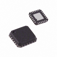
ADL5371ACPZ-R7 Analog Devices Inc, ADL5371ACPZ-R7 Datasheet - Page 3

ADL5371ACPZ-R7
Manufacturer Part Number
ADL5371ACPZ-R7
Description
IC,RF Modulator,LLCC,24PIN,PLASTIC
Manufacturer
Analog Devices Inc
Datasheet
1.ADL5371ACPZ-R7.pdf
(20 pages)
Specifications of ADL5371ACPZ-R7
Design Resources
Interfacing ADL5371 to AD9779A Dual-Channel, 1 GSPS High Speed DAC (CN0017)
Function
Modulator
Lo Frequency
500MHz ~ 1.5GHz
Rf Frequency
500MHz ~ 1.5GHz
P1db
14.4dBm
Noise Floor
-158.6dBm/Hz
Output Power
7.6dBm
Current - Supply
200mA
Voltage - Supply
4.75 V ~ 5.25 V
Test Frequency
900MHz
Package / Case
24-VFQFN, 24-CSP Exposed Pad
Lead Free Status / RoHS Status
Lead free / RoHS Compliant
Other names
ADL5371ACPZ-R7TR
Available stocks
Company
Part Number
Manufacturer
Quantity
Price
Company:
Part Number:
ADL5371ACPZ-R7
Manufacturer:
Bussmann
Quantity:
500
Part Number:
ADL5371ACPZ-R7
Manufacturer:
ADI/亚德诺
Quantity:
20 000
SPECIFICATIONS
V
dc bias; baseband I/Q frequency (f
Table 1.
Parameter
ADL5371
LO INPUTS
BASEBAND INPUTS
POWER SUPPLIES
1
2
Higher LO drive reduces noise at a 6 MHz carrier offset in GSM applications.
See the V-to-I Converter section for architecture information.
S
Output Power, P
Output P1dB
Carrier Feedthrough
Sideband Suppression
Quadrature Error
I/Q Amplitude Balance
Second Harmonic
Third Harmonic
Output IP2
Output IP3
Noise Floor
LO Drive Level
Input Return Loss
I/Q Input Bias Level
Input Bias Current
Input Offset Current
Differential Input Impedance
Bandwidth (0.1 dB)
Bandwidth (1 dB)
Voltage
Supply Current
= 5 V; T
GSM
A
= 25°C; LO = 0 dBm
1
OUT
1
BB
single-ended; baseband I/Q amplitude = 1.4 V p-p differential sine waves in quadrature with a 500 mV
Pin VPS1, Pin VPS2, Pin VPS3, Pin VPS4, and Pin VPS5
Conditions
Low frequency
High frequency
P
P
f1
f1
I/Q inputs = 0 V differential with a 500 mV common-mode bias,
20 MHz carrier offset
6 MHz carrier offset, P
Characterization performed at typical level
See Figure 9 for the return loss vs. frequency plot
Pin IBBP, Pin IBBN, Pin QBBP, Pin QBBN
Current sourcing from each baseband input with a bias of 500 mV dc
) = 1 MHz, LO frequency = 900 MHz, unless otherwise noted.
OUT
OUT
BB
BB
= 3.5 MHz, f2
= 3.5 MHz, f2
− (f
− (f
LO
LO
+ (2 × f
+ (3 × f
BB
BB
BB
BB
)), P
)), P
= 4.5 MHz, P
= 4.5 MHz, P
OUT
OUT
OUT
= 5 dBm, P
= 6.2 dBm
= 6.2 dBm
Rev. 0 | Page 3 of 20
OUT
OUT
= 1.6 dBm per tone
= 1.6 dBm per tone
LO
= 6 dBm, LO = 940 MHz
2
Min
−6
4.75
Typ
500
1500
7.6
14.4
−50
−55
0.1
−0.03
−56
−50
57
27
−158.6
−158.5
0
−7
500
45
0.1
2900
70
350
175
Max
+6
5.25
200
ADL5371
Unit
MHz
MHz
dBm
dBm
dBm
dBc
Degrees
dB
dBc
dBc
dBm
dBm
dBm/Hz
dBc/Hz
dBm
dB
mV
μA
μA
kΩ
MHz
MHz
V
mA


