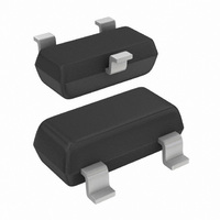
J175,116 NXP Semiconductors, J175,116 Datasheet - Page 5

J175,116
Manufacturer Part Number
J175,116
Description
JFET P-CHAN 30V SOT-54
Manufacturer
NXP Semiconductors
Specifications of J175,116
Package / Case
TO-236-3, SC-59, SOT-23-3
Current - Drain (idss) @ Vds (vgs=0)
7mA @ 15V
Drain To Source Voltage (vdss)
30V
Fet Type
P-Channel
Voltage - Breakdown (v(br)gss)
30V
Voltage - Cutoff (vgs Off) @ Id
3V @ 10nA
Input Capacitance (ciss) @ Vds
8pF @ 10V (VGS)
Resistance - Rds(on)
125 Ohm
Mounting Type
Through Hole
Power - Max
400mW
Configuration
Single
Transistor Polarity
P-Channel
Drain Source Voltage Vds
30 V
Gate-source Breakdown Voltage
30 V
Continuous Drain Current
70 mA
Maximum Operating Temperature
+ 150 C
Minimum Operating Temperature
- 65 C
Mounting Style
SMD/SMT
Lead Free Status / RoHS Status
Lead free / RoHS Compliant
Lead Free Status / RoHS Status
Lead free / RoHS Compliant, Lead free / RoHS Compliant
Other names
934005300116
J175 T/R
J175 T/R
J175 T/R
J175 T/R
PACKAGE OUTLINE
Plastic single-ended leaded (through hole) package; 3 leads
Philips Semiconductors
April 1995
DIMENSIONS (mm are the original dimensions)
Note
1. Terminal dimensions within this zone are uncontrolled to allow for flow of plastic and terminal irregularities.
P-channel silicon field-effect transistors
UNIT
mm
VERSION
OUTLINE
SOT54
D
5.2
5.0
A
0.48
0.40
d
b
E
3
1
2
0.66
0.56
b 1
IEC
b
1
0.45
0.40
c
4.8
4.4
D
JEDEC
TO-92
1.7
1.4
d
REFERENCES
0
4.2
3.6
E
2.54
A
e
SC-43
scale
EIAJ
2.5
5
1.27
e 1
14.5
12.7
5 mm
L
L 1
L 1
2.5
(1)
L
PROJECTION
EUROPEAN
Product specification
J174; J175;
J176; J177
ISSUE DATE
b
97-02-28
c
e 1
e
SOT54


