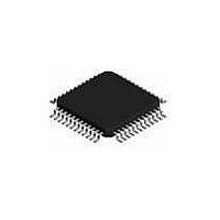
TDA8784HLBE-T NXP Semiconductors, TDA8784HLBE-T Datasheet - Page 13

TDA8784HLBE-T
Manufacturer Part Number
TDA8784HLBE-T
Description
Audio A/D Converter ICs 10BIT A/D INTERFACE CCD CAMERA
Manufacturer
NXP Semiconductors
Datasheet
1.TDA8784HLBE-T.pdf
(28 pages)
Specifications of TDA8784HLBE-T
Conversion Rate
18000 KSPS
Resolution
10 Bit
Operating Supply Voltage
3 V or 5 V
Maximum Operating Temperature
+ 75 C
Minimum Operating Temperature
- 20 C
Package / Case
LQFP-48
Mounting Style
SMD/SMT
Number Of Channels
1
Supply Current
1 mA or 18 mA or 78 mA
Lead Free Status / RoHS Status
Lead free / RoHS Compliant
Other names
TDA8784HL/C4,518
Philips Semiconductors
Table 1 Serial interface programming
Note
1. When CLPADC is HIGH (D4 = 1: serial interface), the ADC input is clamped to voltage level V
Table 2 Standby selection
2002 Oct 23
18 Msps, 10-bit analog-to-digital
interface for CCD cameras
V
A2
ref
0
0
0
0
1
is connected to ground via a capacitance.
ADDRESS BITS
STDBY
A1
0
0
1
1
1
0
0
A0
0
1
0
1
0
OFD output control (D7 to D0).
Cut-off frequency of CDS and AGC. Only the 4 LSBs (D3 to D0) are used for
CDS. D4 to D7 are used for AGC. D8 and D9 should be set to logic 0.
AGC gain control (D8 to D0).
Partial standby controls for power consumption optimization. Only the 4 LSBs
(D3 to D0) are used. Edge control for pulses SHP, SHD, CLAMP and
clock ADC:
Clamp reference DAC (D9 to D0).
D0 = 1: CDS + AGC in standby; I
D1 = 1: OFD DAC in standby; I
D2 = 1: 6 dB amplifier (output on AMPOUT pin) in standby;
I
D3 = 1: SHP and SHD activated with falling edge (for positive pulse)
D4 = 1: CLPDM, CLPOB and CLPADC activated on HIGH level; note 1
D5 = 0: CLKADC activated with falling edge
D6 must be set to logic 0.
CCA
+ I
DATA BITS D9 to D0
CCD
= 95.5 mA
active
LOW
13
DATA BITS D9 to D0
CCA
CCA
+ I
+ I
CCD
CCD
= 95 mA
= 35 mA
I
CCA
+ I
96 mA
4 mA
CCD
ref
Product specification
.
(TYP.)
TDA8784


