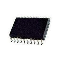
TDA8552TD NXP Semiconductors, TDA8552TD Datasheet - Page 10

TDA8552TD
Manufacturer Part Number
TDA8552TD
Description
Audio Amplifiers AUDIO PWR AMP BTL
Manufacturer
NXP Semiconductors
Datasheet
1.TDA8552TSN1118.pdf
(27 pages)
Specifications of TDA8552TD
Product
Class-AB
Output Power
1.4 W
Available Set Gain
30 dB
Thd Plus Noise
0.1 %
Operating Supply Voltage
5 V
Supply Current
14 mA
Maximum Power Dissipation
2200 mW
Maximum Operating Temperature
+ 85 C
Mounting Style
SMD/SMT
Audio Load Resistance
32 Ohms
Input Offset Voltage
5.5 V
Input Signal Type
Single
Minimum Operating Temperature
- 40 C
Output Signal Type
Differential, Single
Supply Type
Single
Supply Voltage (max)
5.5 V
Supply Voltage (min)
2.7 V
Output Type
2-Channel Stereo
Package / Case
SO-20
Lead Free Status / RoHS Status
Lead free / RoHS Compliant
Other names
TDA8552T/N1,512
NXP Semiconductors
Notes
1. With a load connected at the outputs the quiescent current will increase, the maximum of this increase being equal
2. The DC output voltage with respect to ground is approximately 0.5V
3. Output voltage in mute position is measured with an input of 1 V (RMS) in a bandwidth of 20 kHz, so including noise,
2002 Jan 04
Volume control
t
t
V
V
V
V
I
t
t
Volume attenuator
G
G
N
ΔG
Z
V
W
rep
I(up/down)
wait
rep
i
th(up)
float(max)
float(min)
th(down)
i(max)(rms)
2 x 1.4 W BTL audio amplifiers with digital
volume control and headphone sensing
step
v(l)
v(h)
to
gain select pin is LOW (0 V).
v
SYMBOL
2
×
⎛
⎝
DC output offset voltage
--------------------------------------------------------------- -
pulse width
pulse repetition time
UP/DOWN pin UP threshold
level
UP/DOWN pin floating high
level
UP/DOWN pin floating low
level
UP/DOWN pin DOWN
threshold level
input current UP/DOWN pin
auto repeat wait time
repeat time
low gain; maximum volume
(including power amplifier)
low gain; minimum volume
(including power amplifier)
high gain; maximum volume
(including power amplifier)
high gain; minimum volume
(including power amplifier)
number of gain steps
variation of gain per step
input impedance
maximum input voltage
(RMS value)
R
L
PARAMETER
⎞
⎠
0 < V
key pressed
UP/DOWN
CONDITIONS
10
< V
DD
DD
.
50
100
4.1
−
1.0
0
−
−
−
19
tbf
29
tbf
−
−
14
−
TDA8552T; TDA8552TS
MIN.
−
−
−
−
−
−
−
500
130
20
−60
30
−50
64
1.25
20
−
TYP.
Product specification
−
−
V
3.4
−
0.6
200
−
−
21
tbf
31
tbf
−
−
−
1.75
DD
MAX.
dB
dB
ns
ns
V
V
V
V
μA
ms
ms
dB
dB
dB
kΩ
V
UNIT


