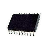
TDA8552TD NXP Semiconductors, TDA8552TD Datasheet - Page 24

TDA8552TD
Manufacturer Part Number
TDA8552TD
Description
Audio Amplifiers AUDIO PWR AMP BTL
Manufacturer
NXP Semiconductors
Datasheet
1.TDA8552TSN1118.pdf
(27 pages)
Specifications of TDA8552TD
Product
Class-AB
Output Power
1.4 W
Available Set Gain
30 dB
Thd Plus Noise
0.1 %
Operating Supply Voltage
5 V
Supply Current
14 mA
Maximum Power Dissipation
2200 mW
Maximum Operating Temperature
+ 85 C
Mounting Style
SMD/SMT
Audio Load Resistance
32 Ohms
Input Offset Voltage
5.5 V
Input Signal Type
Single
Minimum Operating Temperature
- 40 C
Output Signal Type
Differential, Single
Supply Type
Single
Supply Voltage (max)
5.5 V
Supply Voltage (min)
2.7 V
Output Type
2-Channel Stereo
Package / Case
SO-20
Lead Free Status / RoHS Status
Lead free / RoHS Compliant
Other names
TDA8552T/N1,512
NXP Semiconductors
Suitability of surface mount IC packages for wave and reflow soldering methods
Notes
1. All surface mount (SMD) packages are moisture sensitive. Depending upon the moisture content, the maximum
2. These packages are not suitable for wave soldering. On versions with the heatsink on the bottom side, the solder
3. If wave soldering is considered, then the package must be placed at a 45° angle to the solder wave direction.
4. Wave soldering is only suitable for LQFP, TQFP and QFP packages with a pitch (e) equal to or larger than 0.8 mm;
5. Wave soldering is only suitable for SSOP and TSSOP packages with a pitch (e) equal to or larger than 0.65 mm; it is
2002 Jan 04
BGA, HBGA, LFBGA, SQFP, TFBGA
HBCC, HLQFP, HSQFP, HSOP, HTQFP, HTSSOP, HVQFN, SMS
PLCC
LQFP, QFP, TQFP
SSOP, TSSOP, VSO
2 x 1.4 W BTL audio amplifiers with digital
volume control and headphone sensing
temperature (with respect to time) and body size of the package, there is a risk that internal or external package
cracks may occur due to vaporization of the moisture in them (the so called popcorn effect). For details, refer to the
Drypack information in the “Data Handbook IC26; Integrated Circuit Packages; Section: Packing Methods”.
cannot penetrate between the printed-circuit board and the heatsink. On versions with the heatsink on the top side,
the solder might be deposited on the heatsink surface.
The package footprint must incorporate solder thieves downstream and at the side corners.
it is definitely not suitable for packages with a pitch (e) equal to or smaller than 0.65 mm.
definitely not suitable for packages with a pitch (e) equal to or smaller than 0.5 mm.
(3)
, SO, SOJ
PACKAGE
24
not suitable
suitable
not recommended
not recommended
not suitable
WAVE
TDA8552T; TDA8552TS
(2)
SOLDERING METHOD
(3)(4)
(5)
suitable
suitable
suitable
suitable
suitable
Product specification
REFLOW
(1)


