UDA1342TSDB NXP Semiconductors, UDA1342TSDB Datasheet
UDA1342TSDB
Specifications of UDA1342TSDB


Related parts for UDA1342TSDB


UDA1342TSDB Summary of contents
Page 1
DATA SHEET UDA1342TS Audio CODEC Product specification Supersedes data of 2000 Mar 29 INTEGRATED CIRCUITS 2000 Jul 31 ...
Page 2
... NXP Semiconductors Audio CODEC CONTENTS 1 FEATURES 2 APPLICATIONS 3 GENERAL DESCRIPTION 4 QUICK REFERENCE DATA 5 ORDERING INFORMATION 6 BLOCK DIAGRAM 7 PINNING 8 FUNCTIONAL DESCRIPTION 8.1 System clock 8.2 ADC analog front-end 8.2.1 Application with 2 V (RMS) input 8.2.2 Double differential mode 8.3 Decimation filter (ADC) 8.4 Digital mixer (ADC) 8 ...
Page 3
... NXP Semiconductors Audio CODEC 1 FEATURES General • 2.7 to 3.6 V power supply • tolerant digital inputs • High pin compatibility with UDA1341TS • 24 bits data path • Selectable control via L3-bus interface, I interface or static pin control; choice of 2 device 2 addresses in L3-bus and I C-bus mode • ...
Page 4
... NXP Semiconductors Audio CODEC 4 QUICK REFERENCE DATA SYMBOL PARAMETER Supplies V ADC analog supply voltage DDA(ADC) V DAC analog supply voltage DDA(DAC) V digital supply voltage DDD I ADC analog supply current DDA(ADC) I DAC analog supply current DDA(DAC) I digital supply current DDD T ambient temperature amb ...
Page 5
... NXP Semiconductors Audio CODEC SYMBOL PARAMETER Digital-to-analog convertor V output voltage (RMS value) o(rms) (THD+N)/S total harmonic distortion-plus-noise 48 to signal ratio at f (THD+N)/S total harmonic distortion-plus-noise 96 to signal ratio at f S/N signal-to-noise ratio S/N signal-to-noise ratio α channel separation cs Note 1. The output voltage of the DAC is proportionally to the DAC power supply voltage. ...
Page 6
... NXP Semiconductors Audio CODEC 6 BLOCK DIAGRAM V DDA(ADC) handbook, full pagewidth 6 VINL2 2 VINL1 UDA1342TS 18 DATAO 16 BCK DATAI 26 VOUTL V DDA(DAC) 2000 Jul 31 V SSA(ADC) V DDD V SSD PGA ADC ADC PGA ADC ADC DECIMATION FILTER DIGITAL MIXER (ADC) DC-CANCELLATION FILTER DIGITAL INTERFACE DIGITAL MIXER (DAC) ...
Page 7
... NXP Semiconductors Audio CODEC 7 PINNING SYMBOL PIN V 1 analog ground pad SSA(ADC) VINL1 2 analog input pad V 3 analog supply pad DDA(ADC) VINR1 4 analog input pad V 5 analog pad ADCN VINL2 6 analog input pad V 7 analog pad ADCP VINR2 8 analog input pad ...
Page 8
... NXP Semiconductors Audio CODEC handbook, halfpage V SSA(ADC) 1 VINL1 2 V DDA(ADC) 3 VINR1 4 V ADCN 5 VINL2 6 V ADCP 7 UDA1342TS 8 VINR2 IPSEL 9 V DDD 10 V SSD 11 SYSCLK 12 L3MODE 13 L3CLOCK 14 MGT017 Fig.2 Pin configuration. 8 FUNCTIONAL DESCRIPTION 8.1 System clock The UDA1342TS operates in slave mode only, this means that in all applications the system must provide the system clock ...
Page 9
... NXP Semiconductors Audio CODEC 8.2.2 D OUBLE DIFFERENTIAL MODE Since the UDA1342TS is equipped with two stereo ADCs, these two pairs of stereo ADCs can be used to convert a single stereo signal to a signal with a higher performance by using the ADCs in the double differential mode. This mode and the input signals, being channel ...
Page 10
... NXP Semiconductors Audio CODEC handbook, full pagewidth from decimation filter from digital DE-EMPHASIS interface input 8.8 Noise shaper The 5th-order noise shaper operates at 64f in-band quantization noise to frequencies well above the audio band. This noise shaping technique enables high signal-to-noise ratios to be achieved. The noise shaper output is converted into an analog signal using a Filter Stream Digital-to-Analog Converter (FSDAC) ...
Page 11
LEFT WS > BCK DATA MSB B2 MSB S-BUS FORMAT WS LEFT > BCK DATA MSB B2 LSB MSB B2 MSB-JUSTIFIED FORMAT ...
Page 12
... NXP Semiconductors Audio CODEC 8.11 Sampling speed The UDA1342TS operates with sample frequencies from 16 to 110 kHz. This range holds for the CODEC as a whole. The DAC part can be configured in the L3-bus and 2 I C-bus mode to accept 2 times and even 4 times the data speed (e ...
Page 13
... NXP Semiconductors Audio CODEC handbook, halfpage V DDA(DAC) 8.13 Control modes The control mode can be set with pin STATIC and pin L3MODE: • Static pin mode • C-bus mode • L3-bus mode. Table 5 Mode selection PIN STATIC PIN L3MODE − LOW HIGH ...
Page 14
... NXP Semiconductors Audio CODEC 8.14 Static pin mode The controllable features in the static pin mode are: • System clock frequency • Data input and output format select • ADC input channel select. 8.14.1 S YSTEM CLOCK SETTING SELECT In the static pin mode pin L3CLOCK is used to select the system clock setting ...
Page 15
... NXP Semiconductors Audio CODEC Information transfer via the microcontroller bus is organized LSB first and in accordance with the so called ‘L3’ format, in which two different modes of operation can be distinguished: address mode and data transfer mode. Important: • When the device is powered-up, at least one L3CLOCK pulse must be sent to the L3-bus interface to wake-up the interface prior to sending information to the device ...
Page 16
... NXP Semiconductors Audio CODEC 8.15.4 D ATA WRITE MODE The data write format is given in Table 13 and illustrated in Fig.9. When writing data to a device four bytes must be sent: 1. One byte with the device address, being ‘01X0 1000’ where ‘X’ stands for the IPSEL value, including ‘01’ for signalling write to the device ...
Page 17
L3 wake-up pulse after power-up L3CLOCK L3MODE device address 0 1 L3DATA DOM bits Fig.9 Data write mode for L3-bus version 2. L3CLOCK L3MODE device address register address L3DATA DOM bits read prepare read Fig.10 Data read ...
Page 18
... NXP Semiconductors Audio CODEC 2 8.16 I C-bus interface Besides the L3-bus mode the UDA1342TS supports the 2 I C-bus mode; all the features can be controlled by the microcontroller with the same register addresses as used in the L3-bus mode. The exchange of data and control information between the ...
Page 19
W RITE CYCLE The write cycle is used to write data from the microcontroller to the internal registers. The I The device and register addresses are one byte each, data is always two bytes (2-bytes data). The format of ...
Page 20
R EAD CYCLE The read cycle is used to read data from the internal registers of the UDA1342TS to the microcontroller. The I in Table 18. The format of the read cycle is as follows: 1. The microcontroller starts ...
Page 21
REGISTER MAPPING The addresses of the control registers with default values at Power-on reset are shown in Table 19. Functions of the registers are shown in Tables 20 to 45. Table 19 Register map ADDRESS FUNCTION D15 00H system ...
Page 22
... NXP Semiconductors Audio CODEC 9.1 Reset A 1-bit value to initialize the L3-bus and I except the system register (00H) with default settings by setting bit RST = 1. Table 20 Reset bit RST 0 no reset 1 reset registers to default 9.2 Quick mode switch A 1-bit value to enable the quick mode change of the ADC. ...
Page 23
... NXP Semiconductors Audio CODEC 9.8 Data format A 3-bit value to select the data format. Table 27 Data format selection IF2 IF1 IF0 2 S-bus LSB-justified16 bits LSB-justified 20 bits LSB-justified 24 bits MSB-justified LSB-justified 16 bits input and MSB-justified output LSB-justified 20 bits input and MSB-justified output LSB-justified 24 bits input and MSB-justified output 9 ...
Page 24
... NXP Semiconductors Audio CODEC Table 32 Input oversampling rate OS1 OS0 MODE 0 0 single speed 0 1 double speed 1 0 quad speed 1 1 reserved 9.14 Silence detection period A 2-bit value to define the silence period for the silence detector. Table 33 Silence detection period SD1 ...
Page 25
... NXP Semiconductors Audio CODEC Table 36 Bass boost settings BB3 BB2 BB1 BB0 9.18 Treble A 2-bit value to program the treble setting. The used set depends on the setting of bits M1 and M0 the −3 dB point for minimum setting is 3.0 kHz and the −3 dB point for maximum setting is 1.5 kHz. The default value is 00 ...
Page 26
... NXP Semiconductors Audio CODEC Table 41 De-emphasis settings DE2 DE1 DE0 de-emphasis de-emphasis de-emphasis de-emphasis de-emphasis at f 9.23 ADC input amplifier gain Two 4-bit values to program the gain of the input amplifiers. Bits IA applies for input amplifier A and bits IB to input amplifier B. Table 42 ADC input amplifier gain settings ...
Page 27
... NXP Semiconductors Audio CODEC 9.24 DAC volume control Four 8-bit values to program the volume attenuations. The range is from 0 to −66 dB and −∞ steps of 0.25 dB. Bits VL and VR are master volumes for the left and right channels. Table 43 DAC volume settings VL7 ...
Page 28
... NXP Semiconductors Audio CODEC Table 44 DAC volume settings VA7 VA6 VA5 VB7 VB6 VB5 9.26 ADC mixer gain control Two 8-bit values to program the channel 1 and 2 mixing, when the mixer mode is selected. Bits MA applies to channel 1 and bits MB to channel 2. The range is from +24 to −63.5 dB and −∞ steps of 0.5 dB. ...
Page 29
... NXP Semiconductors Audio CODEC MA7 MA6 MA5 MB7 MB6 MB5 2000 Jul 31 MA4 MA3 MA2 MB4 MB3 MB2 Product specification UDA1342TS MA1 MA0 MIXER GAIN (dB) MB1 MB0 −63.0 −63.5 −∞ ...
Page 30
... NXP Semiconductors Audio CODEC 10 LIMITING VALUES In accordance with the Absolute Maximum Rating System (IEC 60134). SYMBOL PARAMETER V supply voltage DD T maximum crystal temperature xtal(max) T storage temperature stg T ambient temperature amb V electrostatic handling voltage es I latch-up protection current lu(prot) I short-circuit current of DAC ...
Page 31
... NXP Semiconductors Audio CODEC SYMBOL PARAMETER I ADC analog supply current DDA(ADC) I DAC analog supply current DDA(DAC) I digital supply current DDD Digital input pins (5 V tolerant TTL compatible) V HIGH-level input voltage IH V LOW-level input voltage IL ⎪I ⎪ input leakage current LI C input capacitance ...
Page 32
... NXP Semiconductors Audio CODEC 15 AC CHARACTERISTICS 3 DDD DDA(ADC) DDA(DAC) to ground; unless otherwise specified. SYMBOL PARAMETER Analog-to-digital converter V input voltage i(rms) (RMS value) ΔV unbalance between i channels (THD + N)/S total harmonic 48 distortion-plus-noise to signal ratio at f 2000 Jul kHz at −1 dB ° amb CONDITIONS ...
Page 33
... NXP Semiconductors Audio CODEC SYMBOL PARAMETER (THD + N)/S total harmonic 96 distortion-plus-noise to signal ratio at f S/N signal-to-noise ratio kHz s S/N signal-to-noise ratio kHz s α channel separation cs PSRR power supply rejection ratio Digital-to-analog converter V output voltage o(rms) (RMS value) ΔV unbalance between o channels ...
Page 34
... NXP Semiconductors Audio CODEC 16 TIMING 2 DDD DDA(ADC) DDA(DAC) specified. SYMBOL PARAMETER System clock timing; note 1 (see Fig.11) T system clock cycle time sys t system clock LOW time CWL SYMBOL PARAMETER t system clock HIGH time CWH Serial interface input/output data timing (see Fig.12) ...
Page 35
... NXP Semiconductors Audio CODEC SYMBOL PARAMETER t L3MODE set-up time in data su(L3)D transfer mode t L3MODE hold time in data h(L3)D transfer mode t L3MODE stop time in data stp(L3) transfer mode t L3DATA set-up time in address su(L3)DA and data transfer mode t L3DATA hold time in address and ...
Page 36
CWH handbook, full pagewidth t CWL T sys Fig.11 Timing of system clock. handbook, full pagewidth WS t BCKH BCK t BCKL T cy(BCK) DATAO DATAI Fig.12 Serial interface input data timing. MGR984 t d(DATAO-BCK) ...
Page 37
... NXP Semiconductors Audio CODEC handbook, full pagewidth L3MODE t h(L3)A L3CLOCK L3DATA handbook, full pagewidth L3MODE t su(L3)D L3CLOCK L3DATA write L3DATA read 2000 Jul 31 t CLK(L3)L t CLK(L3)H t su(L3)A t su(L3)DA BIT 0 Fig.13 Timing of address mode. t CLK(L3)L t CLK(L3)H t su(L3)DA t h(L3)DA BIT 0 Fig.14 Timing of data transfer mode for write and read. ...
Page 38
SDA t BUF t LOW t r SCL t HD;STA t HD;DAT SU;STA t HIGH t SU;DAT Sr 2 Fig.15 Timing of the I C-bus transfer. t HD;STA SU;STO P MBC611 ...
Page 39
... NXP Semiconductors Audio CODEC 17 APPLICATION INFORMATION L1 handbook, full pagewidth +3 V BLM32A07 L2 BLM32A07 C12 100 μF ground ( R13 system clock 47 Ω S-bus C1 left 47 μF input 1 ( right 47 μF ( left 47 μF (16 V) input 2 C4 right 47 μF (16 V) L3-bus 2 I C-bus 2000 Jul 31 V DDA ...
Page 40
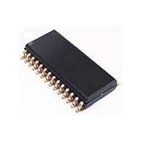
... NXP Semiconductors Audio CODEC 18 PACKAGE OUTLINE SSOP28: plastic shrink small outline package; 28 leads; body width 5 pin 1 index 1 e DIMENSIONS (mm are the original dimensions) A UNIT max. 0.21 1. 0.25 0.05 1.65 Note 1. Plastic or metal protrusions of 0.2 mm maximum per side are not included. OUTLINE ...
Page 41
... NXP Semiconductors Audio CODEC 19 SOLDERING 19.1 Introduction to soldering surface mount packages This text gives a very brief insight to a complex technology. A more in-depth account of soldering ICs can be found in our “Data Handbook IC26; Integrated Circuit Packages” (document order number 9398 652 90011). ...
Page 42
... NXP Semiconductors Audio CODEC 19.5 Suitability of surface mount IC packages for wave and reflow soldering methods PACKAGE BGA, LFBGA, SQFP, TFBGA HBCC, HLQFP, HSQFP, HSOP, HTQFP, HTSSOP, SMS (3) PLCC , SO, SOJ LQFP, QFP, TQFP SSOP, TSSOP, VSO Notes 1. All surface mount (SMD) packages are moisture sensitive. Depending upon the moisture content, the maximum temperature (with respect to time) and body size of the package, there is a risk that internal or external package cracks may occur due to vaporization of the moisture in them (the so called popcorn effect) ...
Page 43
... In no event shall NXP Semiconductors be liable for any indirect, incidental, punitive, special or consequential damages (including - without limitation - lost profits, lost savings, business interruption, costs related to the ...
Page 44
... NXP Semiconductors’ specifications such use shall be solely at customer’s own risk, and (c) customer fully indemnifies NXP Semiconductors for any liability, damages or failed product claims resulting from customer design and use of the product for automotive applications beyond NXP Semiconductors’ ...
Page 45
... Interface, Security and Digital Processing expertise Customer notification This data sheet was changed to reflect the new company name NXP Semiconductors, including new legal definitions and disclaimers. No changes were made to the technical content, except for package outline drawings which were updated to the latest version. ...