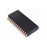
UDA1342TSDB NXP Semiconductors, UDA1342TSDB Datasheet - Page 16

UDA1342TSDB
Manufacturer Part Number
UDA1342TSDB
Description
Audio CODECs AUDIO CODEC MINIDISC
Manufacturer
NXP Semiconductors
Datasheet
1.UDA1342TSN1512.pdf
(45 pages)
Specifications of UDA1342TSDB
Number Of Adc Inputs
4
Number Of Dac Outputs
2
Conversion Rate
110 KSPs
Interface Type
Serial (I2C), L3
Resolution
24 bit
Operating Supply Voltage
2.7 V to 3.6 V
Maximum Operating Temperature
+ 85 C
Mounting Style
SMD/SMT
Package / Case
SSOP-28
Minimum Operating Temperature
- 40 C
Number Of Channels
6
Snr
100 dB
Supply Current
20 mA
Lead Free Status / RoHS Status
Lead free / RoHS Compliant
Other names
UDA1342TS/N1,512
NXP Semiconductors
8.15.4
The data write format is given in Table 13 and illustrated
in Fig.9.
When writing data to a device four bytes must be sent:
1. One byte with the device address, being ‘01X0 1000’
2. One byte starting with a logic 0 for signalling write
3. One byte which is the Most Significant Data (MSD)
4. One byte which is the Least Significant Data (LSD)
8.15.5
The data write format is given in Table 14 and illustrated
in Fig.10.
When reading from the device, a prepare read must first be
done. After the prepare read, the device address is sent
again. The device then returns with the register address,
indicating whether the address was valid or not, and the
data of the register.
Table 13 L3-bus format for data write
Table 14 L3-bus format for prepare read and read data
2000 Jul 31
Address
Data transfer 1
Data transfer 2
Data transfer 3
Prepare read
Address
Data transfer 1
Read data
Address
Data transfer 1
Data transfer 2
Data transfer 3
Audio CODEC
where ‘X’ stands for the IPSEL value, including ‘01’ for
signalling write to the device.
followed by 7 bits indicating the register address.
byte 1.
byte 2.
L3MODE
L3MODE
D
D
ATA WRITE MODE
ATA READ MODE
device address
register address
MSD byte 1
LSD byte 2
device address
register address
device address
register address
MSD byte 1
LSD byte 2
DATA TYPE
DATA TYPE
FIRST IN TIME
FIRST IN TIME
BIT 0
BIT 0
D15
D15
D7
0/1
D7
0
0
0
1
1
BIT 1
BIT 1
D14
D14
D6
D6
A6
A6
A6
1
1
1
16
The data read mode is explained below:
1. One byte with the device address, being ‘01X0 1000’
2. One byte is sent with the register address which needs
3. One byte with the device address including ‘11’ is sent
4. The device now writes the requested register address
5. The device writes data from the requested register to
IPSEL
IPSEL
IPSEL
BIT 2
BIT 2
where ‘X’ stands for the IPSEL value, including ‘01’ for
signalling write to the device.
to be read. This byte starts with a logic 1, which
indicates that there will be a read action from the
register.
to the device. The ‘11’ indicates that the device must
write data to the microcontroller.
on the L3-bus, indicating whether the requested
register was valid (logic 0) or invalid (logic 1).
the L3-bus with the MSD byte 1 first, followed by the
LSD byte 2.
D13
D13
D5
D5
A5
A5
A5
BIT 3
BIT 3
D12
D12
D4
D4
A4
A4
A4
0
0
0
BIT 4
BIT 4
D11
D11
D3
D3
A3
A3
A3
1
1
1
BIT 5
BIT 5
D10
D10
D2
D2
A2
A2
A2
0
0
0
UDA1342TS
Product specification
LAST IN TIME
BIT 6
LAST IN TIME
BIT 6
D9
D1
D9
D1
A1
A1
A1
0
0
0
BIT 7
BIT 7
D8
D0
D8
D0
A0
A0
A0
0
0
0


