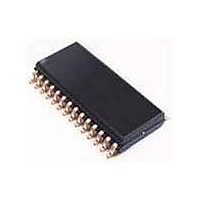
PCK2001MDB NXP Semiconductors, PCK2001MDB Datasheet - Page 10

PCK2001MDB
Manufacturer Part Number
PCK2001MDB
Description
Clock Buffer PII CLCK DRVR MOBILE
Manufacturer
NXP Semiconductors
Datasheet
1.PCK2001MDB118.pdf
(14 pages)
Specifications of PCK2001MDB
Mounting Style
SMD/SMT
Package / Case
SOT-341
Lead Free Status / RoHS Status
Lead free / RoHS Compliant
Other names
PCK2001MDB,112
Available stocks
Company
Part Number
Manufacturer
Quantity
Price
Company:
Part Number:
PCK2001MDB
Manufacturer:
PHILIPS
Quantity:
40
Part Number:
PCK2001MDB
Manufacturer:
NXP/恩智浦
Quantity:
20 000
1. Inactive means outputs are held LOW and are disabled from switching. These outputs are designed to be configured at power-on and are
1. Inactive means outputs are held LOW and are disabled from switching. These outputs are designed to be configured at power-on and are
1. Inactive means outputs are held LOW and are disabled from switching. These outputs are designed to be configured at power-on and are
Philips Semiconductors
SERIAL CONFIGURATION MAP
The serial bits will be read by the clock buffer in the following order:
All unused register bits (Reserved and N/A) should be desined as “Don’t Care”. It is expected that the controller will force all of these bits to a
“0” level.
All register bits labeled “Initialize to 0” must be written to zero during intialization. Failure to do so may result in a higher than normal operating
current. The controller will read back the last written value.
Byte 0: Output active/inactive register
1 = enable; 0 = disable
NOTE:
Byte 1: Output active/inactive register
1 = enable; 0 = disable
NOTE:
Byte 2: Optional register for possible future requirments
NOTE:
2000 May 17
14.318–150 MHz I
Byte 0 – Bits 7, 6, 5, 4, 3, 2, 1, 0
Byte 1 – Bits 7, 6, 5, 4, 3, 2, 1, 0
Byte 2 – Bits 7, 6, 5, 4, 3, 2, 1, 0
not expected to be configured during the normal modes of operation.
not expected to be configured during the normal modes of operation.
not expected to be configured during the normal modes of operation.
BIT
BIT
BIT
7
6
5
4
3
2
1
0
7
6
5
4
3
2
1
0
7
6
5
4
3
2
1
0
PIN#
PIN#
PIN#
27
26
23
22
18
—
—
—
—
—
—
—
—
11
—
—
—
—
—
—
7
6
3
2
2
C 1:10 clock buffer
BUF_OUT15
BUF_OUT14
BUF_OUT13
BUF_OUT12
BUF_OUT11
BUF_OUT10
BUF_OUT17
BUF_OUT16
BUF_OUT7
BUF_OUT6
BUF_OUT5
BUF_OUT4
BUF_OUT3
BUF_OUT2
BUF_OUT1
BUF_OUT0
BUF_OUT9
BUF_OUT8
(reserved)
(reserved)
(reserved)
(reserved)
(reserved)
(reserved)
NAME
NAME
NAME
10
DESCRIPTION
DESCRIPTION
DESCRIPTION
Active/Inactive
Active/Inactive
Active/Inactive
Active/Inactive
Active/Inactive
Active/Inactive
Active/Inactive
Active/Inactive
Active/Inactive
Active/Inactive
Initialize to 0
Initialize to 0
Initialize to 0
Initialize to 0
Initialize to 0
Initialize to 0
Initialize to 0
Initialize to 0
(reserved)
(reserved)
(reserved)
(reserved)
(reserved)
(reserved)
PCK2001M
Product specification


