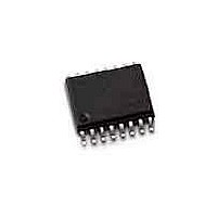
M41T94MQ6 STMicroelectronics, M41T94MQ6 Datasheet - Page 15

M41T94MQ6
Manufacturer Part Number
M41T94MQ6
Description
Real Time Clock Serial 512 (64x8)
Manufacturer
STMicroelectronics
Datasheet
1.M41T94MQ6TR.pdf
(41 pages)
Specifications of M41T94MQ6
Function
Clock, Calendar, Alarm, Timer Interrupt
Rtc Memory Size
64 B
Supply Voltage (max)
5.5 V
Supply Voltage (min)
2.7 V
Maximum Operating Temperature
+ 85 C
Minimum Operating Temperature
- 40 C
Mounting Style
SMD/SMT
Rtc Bus Interface
Serial
Package / Case
SO-16
Time Format
HH:MM:SS:hh
Lead Free Status / RoHS Status
Lead free / RoHS Compliant
Available stocks
Company
Part Number
Manufacturer
Quantity
Price
Company:
Part Number:
M41T94MQ6
Manufacturer:
ST
Quantity:
5 510
Company:
Part Number:
M41T94MQ6
Manufacturer:
RECOM
Quantity:
5 510
Company:
Part Number:
M41T94MQ6E
Manufacturer:
ST
Quantity:
5 892
Part Number:
M41T94MQ6E
Manufacturer:
ST
Quantity:
20 000
Company:
Part Number:
M41T94MQ6F
Manufacturer:
ST
Quantity:
5 892
Company:
Part Number:
M41T94MQ6F
Manufacturer:
ST
Quantity:
4 960
Part Number:
M41T94MQ6F
Manufacturer:
ST
Quantity:
20 000
M41T94
3.2
Note:
3.3
Read and write cycles
Address and data are shifted MSB first into the serial data input (SDI) and out of the serial
data output (SDO). Any data transfer considers the first bit to define whether a READ or
WRITE will occur. This is followed by seven bits defining the address to be read or written.
Data is transferred out of the SDO for a READ operation and into the SDI for a WRITE
operation. The address is always the second through the eighth bit written after the Enable
(E) pin goes low. If the first bit is a '1,' one or more WRITE cycles will occur. If the first bit is a
'0,' one or more READ cycles will occur (see Figure
page
Data transfers can occur one byte at a time or in multiple byte burst mode, during which the
address pointer will be automatically incremented. For a single byte transfer, one byte is
read or written and then E is driven high. For a multiple byte transfer all that is required is
that E continue to remain low. Under this condition, the address pointer will continue to
increment as stated previously. Incrementing will continue until the device is deselected by
taking E high. The address will wrap to 00h after incrementing to 3Fh.
The system-to-user transfer of clock data will be halted whenever the address being read is
a clock address (00h to 07h). Although the clock continues to maintain the correct time, this
will prevent updates of time and date during either a READ or WRITE of these address
locations by the user. The update will resume either due to a deselect condition or when the
pointer increments to an non-clock or RAM address (08h to 3Fh).
This is true both in READ and WRITE mode.
Data retention mode
With valid V
WRITE cycles. Should the supply voltage decay, the M41T94 will automatically deselect,
write protecting itself when V
page
returns to nominal levels. When V
switched from the V
time, and the clock registers are maintained from the attached battery supply. All outputs
become high impedance. On power-up, when V
protection continues for t
during this time (see
be taken high for at least t
For a further more detailed review of battery lifetime calculations, please see application
note AN1012.
16).
31). At this time, the reset pin (RST) is driven active and will remain active until V
CC
applied, the M41T94 can be accessed as described above with READ or
CC
Figure 17 on page
pin to the SNAPHAT battery (or external battery for SO16) at this
REC
EHEL
CC
by internally inhibiting E. The RST signal also remains active
, then low.
falls between V
CC
falls below the switchover voltage (V
31). Before the next active cycle, chip enable should
PFD
CC
returns to a nominal value, write
(max) and V
Figure 9 on page 16
PFD
(min) (see
SO
and
), power input is
Figure 10 on
Figure 17 on
Operation
CC
15/41


