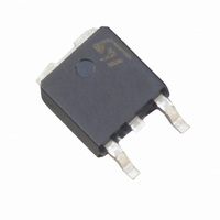
STD90N02L STMicroelectronics, STD90N02L Datasheet - Page 9

STD90N02L
Manufacturer Part Number
STD90N02L
Description
MOSFET N-CH 25V 60A DPAK
Manufacturer
STMicroelectronics
Series
STripFET™r
Datasheet
1.STD90N02L.pdf
(17 pages)
Specifications of STD90N02L
Fet Type
MOSFET N-Channel, Metal Oxide
Fet Feature
Logic Level Gate
Rds On (max) @ Id, Vgs
6 mOhm @ 30A, 10V
Drain To Source Voltage (vdss)
25V
Current - Continuous Drain (id) @ 25° C
60A
Vgs(th) (max) @ Id
1.8V @ 250µA
Gate Charge (qg) @ Vgs
22nC @ 5V
Input Capacitance (ciss) @ Vds
2050pF @ 16V
Power - Max
70W
Mounting Type
Surface Mount
Package / Case
DPak, TO-252 (2 leads+tab), SC-63
Lead Free Status / RoHS Status
Lead free / RoHS Compliant
Other names
497-7978-2
STD90N02L
STD90N02L
Available stocks
Company
Part Number
Manufacturer
Quantity
Price
STD90N02L - STD90N02L-1
3
Buck converter
The power losses associated with the FETs in a Synchronous Buck converter can be
estimated using the equations shown in the table below. The formulas give a good
approximation, for the sake of performance comparison, of how different pairs of devices
affect the converter efficiency. However a very important parameter, the working
temperature, is not considered. The real device behavior is really dependent on how the
heat generated inside the devices is removed to allow for a safer working junction
temperature.
The low side (SW2) device requires:
Very low R
Small Q
Small C
Small Q
The C
avoid the cross conduction phenomenon.
The high side (SW1) device requires:
Small R
gate
Small Q
Low R
Figure 15. Synchronous buck converter
gd
DS(on)
OSS
G
GLS
rr
G
/C
to reduce losses on SW1 during its turn-on
and L
to have a faster commutation and to reduce gate charge losses
gs
DS(on)
to reduce the gate charge losses
to reduce losses due to output capacitance
to reduce the conduction losses
ratio lower than Vth/Vgg ratio especially with low drain to source voltage to
G
to reduce conduction losses
to allow higher gate current peak and to limit the voltage feedback on the
Buck converter
9/17


