PHB21N06LT,118 NXP Semiconductors, PHB21N06LT,118 Datasheet - Page 2
PHB21N06LT,118
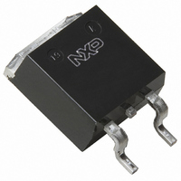
Manufacturer Part Number
PHB21N06LT,118
Description
MOSFET N-CH 55V 19A SOT404
Manufacturer
NXP Semiconductors
Series
TrenchMOS™r
Datasheet
1.PHB21N06LT118.pdf
(11 pages)
Specifications of PHB21N06LT,118
Package / Case
D²Pak, TO-263 (2 leads + tab)
Mounting Type
Surface Mount
Power - Max
56W
Fet Type
MOSFET N-Channel, Metal Oxide
Gate Charge (qg) @ Vgs
9.4nC @ 5V
Vgs(th) (max) @ Id
2V @ 1mA
Current - Continuous Drain (id) @ 25° C
19A
Drain To Source Voltage (vdss)
55V
Fet Feature
Logic Level Gate
Rds On (max) @ Id, Vgs
70 mOhm @ 10A, 10V
Minimum Operating Temperature
- 55 C
Configuration
Single
Transistor Polarity
N-Channel
Resistance Drain-source Rds (on)
0.07 Ohm @ 10 V
Drain-source Breakdown Voltage
55 V
Gate-source Breakdown Voltage
+/- 15 V
Continuous Drain Current
19 A
Power Dissipation
56000 mW
Maximum Operating Temperature
+ 175 C
Mounting Style
SMD/SMT
Lead Free Status / RoHS Status
Lead free / RoHS Compliant
Lead Free Status / RoHS Status
Lead free / RoHS Compliant, Lead free / RoHS Compliant
Other names
934054570118::PHB21N06LT /T3::PHB21N06LT /T3


Philips Semiconductors
AVALANCHE ENERGY LIMITING VALUES
Limiting values in accordance with the Absolute Maximum System (IEC 134)
THERMAL RESISTANCES
ELECTRICAL CHARACTERISTICS
T
August 1999
N-channel TrenchMOS
Logic level FET
SYMBOL PARAMETER
E
I
SYMBOL PARAMETER
R
R
SYMBOL PARAMETER
V
V
R
g
I
I
Q
Q
Q
t
t
t
t
L
L
L
C
C
C
j
AS
= 25˚C unless otherwise specified
GSS
DSS
d on
r
d off
f
fs
d
d
s
AS
(BR)DSS
GS(TO)
th j-mb
th j-a
DS(ON)
iss
oss
rss
g(tot)
gs
gd
Non-repetitive avalanche
energy
Peak non-repetitive
avalanche current
Thermal resistance junction
to mounting base
Thermal resistance junction
to ambient
Drain-source breakdown
voltage
Gate threshold voltage
Drain-source on-state
resistance
Forward transconductance
Gate source leakage current V
Zero gate voltage drain
current
Total gate charge
Gate-source charge
Gate-drain (Miller) charge
Turn-on delay time
Turn-on rise time
Turn-off delay time
Turn-off fall time
Internal drain inductance
Internal drain inductance
Internal source inductance
Input capacitance
Output capacitance
Feedback capacitance
transistor
CONDITIONS
Unclamped inductive load, I
t
V
fig:15
CONDITIONS
SOT78 package, in free air
SOT428 and SOT404 package, pcb
mounted, minimum footprint
CONDITIONS
V
V
V
V
V
V
I
V
R
Resistive load
Measured from tab to centre of die
Measured from drain lead to centre of die
(SOT78 package only)
Measured from source lead to source
bond pad
V
p
D
DD
GS
DS
GS
GS
DS
GS
DS
DD
GS
G
= 20 A; V
= 100 s; T
= 10 ; V
= 0 V; I
= V
= 10 V; I
= 5 V; I
= 25 V; I
= 5 V; V
= 55 V; V
= 30 V; R
= 0 V; V
25 V; R
GS
; I
D
D
D
DD
DS
D
D
GS
= 0.25 mA;
= 1 mA
= 10 A
j
DS
GS
GS
= 44 V; V
D
= 10 A
= 10 A
prior to avalanche = 25˚C;
2
= 25 V; f = 1 MHz
= 1.2 ;
= 5 V
= 0 V
= 0 V;
= 50 ; V
GS
= 5 V
GS
AS
= 5 V; refer to
= 9.7 A;
T
T
T
PHP21N06LT, PHB21N06LT
T
T
j
j
j
j
j
= 175˚C
= 175˚C
= 175˚C
= -55˚C
= -55˚C
MIN.
1.0
0.5
TYP.
55
50
MIN.
5
-
-
-
-
-
-
-
-
-
-
-
-
-
-
-
-
-
-
-
-
60
50
-
-
-
TYP. MAX. UNIT
0.05
Product specification
466
PHD21N06LT
1.5
9.4
2.2
5.4
3.5
4.5
7.5
55
60
13
10
88
25
25
95
71
7
-
-
-
-
-
-
MAX.
MAX.
2.7
34
19
-
-
158
100
500
120
650
135
2.0
2.3
70
75
10
15
40
45
85
-
-
-
-
-
-
-
-
-
-
Rev 1.500
UNIT
UNIT
K/W
K/W
K/W
mJ
A
m
m
m
nA
nC
nC
nC
nH
nH
nH
pF
pF
pF
ns
ns
ns
ns
V
V
V
V
V
S
A
A
Related parts for PHB21N06LT,118
Image
Part Number
Description
Manufacturer
Datasheet
Request
R

Part Number:
Description:
NXP Semiconductors designed the LPC2420/2460 microcontroller around a 16-bit/32-bitARM7TDMI-S CPU core with real-time debug interfaces that include both JTAG andembedded trace
Manufacturer:
NXP Semiconductors
Datasheet:

Part Number:
Description:
NXP Semiconductors designed the LPC2458 microcontroller around a 16-bit/32-bitARM7TDMI-S CPU core with real-time debug interfaces that include both JTAG andembedded trace
Manufacturer:
NXP Semiconductors
Datasheet:
Part Number:
Description:
NXP Semiconductors designed the LPC2468 microcontroller around a 16-bit/32-bitARM7TDMI-S CPU core with real-time debug interfaces that include both JTAG andembedded trace
Manufacturer:
NXP Semiconductors
Datasheet:
Part Number:
Description:
NXP Semiconductors designed the LPC2470 microcontroller, powered by theARM7TDMI-S core, to be a highly integrated microcontroller for a wide range ofapplications that require advanced communications and high quality graphic displays
Manufacturer:
NXP Semiconductors
Datasheet:
Part Number:
Description:
NXP Semiconductors designed the LPC2478 microcontroller, powered by theARM7TDMI-S core, to be a highly integrated microcontroller for a wide range ofapplications that require advanced communications and high quality graphic displays
Manufacturer:
NXP Semiconductors
Datasheet:
Part Number:
Description:
The Philips Semiconductors XA (eXtended Architecture) family of 16-bit single-chip microcontrollers is powerful enough to easily handle the requirements of high performance embedded applications, yet inexpensive enough to compete in the market for hi
Manufacturer:
NXP Semiconductors
Datasheet:
Part Number:
Description:
The XA-S3 device is a member of Philips Semiconductors? XA(eXtended Architecture) family of high performance 16-bitsingle-chip microcontrollers
Manufacturer:
NXP Semiconductors
Datasheet:

Part Number:
Description:
The NXP BlueStreak LH75401/LH75411 family consists of two low-cost 16/32-bit System-on-Chip (SoC) devices
Manufacturer:
NXP Semiconductors
Datasheet:
Part Number:
Description:
The NXP LPC3130/3131 combine an 180 MHz ARM926EJ-S CPU core, high-speed USB2
Manufacturer:
NXP Semiconductors
Datasheet:
Part Number:
Description:
The NXP LPC3141 combine a 270 MHz ARM926EJ-S CPU core, High-speed USB 2
Manufacturer:
NXP Semiconductors
Part Number:
Description:
The NXP LPC3143 combine a 270 MHz ARM926EJ-S CPU core, High-speed USB 2
Manufacturer:
NXP Semiconductors

Part Number:
Description:
The NXP LPC3152 combines an 180 MHz ARM926EJ-S CPU core, High-speed USB 2
Manufacturer:
NXP Semiconductors
Part Number:
Description:
The NXP LPC3154 combines an 180 MHz ARM926EJ-S CPU core, High-speed USB 2
Manufacturer:
NXP Semiconductors

Part Number:
Description:
Standard level N-channel enhancement mode Field-Effect Transistor (FET) in a plastic package using NXP High-Performance Automotive (HPA) TrenchMOS technology
Manufacturer:
NXP Semiconductors
Datasheet: