STQ3NK50ZR-AP STMicroelectronics, STQ3NK50ZR-AP Datasheet
STQ3NK50ZR-AP
Specifications of STQ3NK50ZR-AP


Related parts for STQ3NK50ZR-AP


STQ3NK50ZR-AP Summary of contents
Page 1
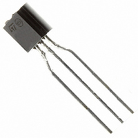
... STD3NK50Z-1 January 2005 STD3NK50Z - STD3NK50Z-1 Zener-Protected SuperMESH™ MOSFET Figure 1: Package DS(on) D 3.3 0 3.3 2 3.3 2 TO-92 (Ammopak) Figure 2: Internal Schematic Diagram MARKING PACKAGE Q3NK50ZR D3NK50Z D3NK50Z STQ3NK50ZR- IPAK PACKAGING TO-92 AMMOPAK DPAK TAPE & REEL IPAK 3 1 DPAK 3 TUBE Rev. 2 1/14 ...
Page 2
... STD3NK50Z - STD3NK50Z-1 - STQ3NK50ZR-AP Table 3: Absolute Maximum ratings Symbol V Drain-source Voltage ( Drain-gate Voltage (R DGR V Gate- source Voltage GS I Drain Current (continuous Drain Current (continuous Drain Current (pulsed Total Dissipation at T TOT Derating Factor V Gate source ESD (HBM-C=100 pF, R= 1.5K ESD(G-S) dv/dt (1) Peak Diode Recovery voltage slope ...
Page 3
... Reverse Recovery Current RRM Note: 1. Pulsed: Pulse duration = 300 µs, duty cycle 1 Pulse width limited by safe operating area defined as a constant equivalent capacitance giving the same charging time as C oss eq DSS STD3NK50Z - STD3NK50Z-1 - STQ3NK50ZR-AP =25°C UNLESS OTHERWISE SPECIFIED) CASE Test Conditions mA ...
Page 4
... STD3NK50Z - STD3NK50Z-1 - STQ3NK50ZR-AP Figure 3: Safe Operating Area For TO-92 Figure 4: Safe Operating Area For DPAK / IPAK Figure 5: Output Characteristics 4/14 Figure 6: Thermal Impedance TO-92 Figure 7: Thermal Impedance For DPAK / IPAK Figure 8: Transfer Characteristics ...
Page 5
... Figure 9: Transconductance Figure 10: Gate Charge vs Gate-source Voltage Figure 11: Static Drain-Source On Resistance STD3NK50Z - STD3NK50Z-1 - STQ3NK50ZR-AP Figure 12: Capacitance Variations Figure 13: Normalized Gate Threshold Voltage vs Temperature Figure 14: Source-Drain Forward Characteris- tics 5/14 ...
Page 6
... STD3NK50Z - STD3NK50Z-1 - STQ3NK50ZR-AP Figure 15: Maximum Avalanche Energy vs Temperature Figure 16: Normalized On Resistance vs Tem- perature 6/14 Figure 17: Normalized BV DSS vs Temperature ...
Page 7
... Figure 18: Unclamped Inductive Load Test Cir- cuit Figure 19: Switching Times Test Circuit For Resistive Load Figure 20: Test Circuit For Inductive Load Switching and Diode Recovery Times STD3NK50Z - STD3NK50Z-1 - STQ3NK50ZR-AP Figure 21: Unclamped Inductive Wafeform Figure 22: Gate Charge Test Circuit 7/14 ...
Page 8
... STD3NK50Z - STD3NK50Z-1 - STQ3NK50ZR-AP DIM. MIN. A 2.20 A1 0.90 A2 0.03 B 0.64 B2 5.20 C 0.45 C2 0.48 D 6.00 E 6.40 G 4. 8/14 TO-252 (DPAK) MECHANICAL DATA mm TYP. MAX. 2.40 1.10 0.23 0.90 5.40 0.60 0.60 6.20 6.60 4.60 10.10 0.8 1. inch MIN. TYP. MAX. 0.087 0.094 ...
Page 9
... B 0. 0. 6.4 G 4 0 STD3NK50Z - STD3NK50Z-1 - STQ3NK50ZR-AP inch MAX. MIN. TYP. 2.4 0.086 1.1 0.035 1.3 0.027 0.9 0.025 5.4 0.204 0.85 0.012 0.95 0.6 0.017 0.6 0.019 6.2 0.236 6.6 0.252 4.6 0.173 16.3 ...
Page 10
... STD3NK50Z - STD3NK50Z-1 - STQ3NK50ZR-AP DIM. MIN. A 4.32 b 0.36 D 4.45 E 3.30 e 2.41 e1 1.14 L 12.70 R 2.16 S1 0.92 W 0.41 V 10/14 TO-92 MECHANICAL DATA mm. TYP MAX. MIN. 4.95 0.170 0.51 0.014 4.95 0.175 3.94 0.130 2.67 0.094 1.40 0.044 15.49 0.50 2.41 0.085 1.52 0.036 0.56 0.016 5° ...
Page 11
... P1 7.9 8.1 0.311 0.319 P2 1.9 2.1 0.075 0.082 R 40 1.574 W 15.7 16.3 0.618 0.641 * on sales type STD3NK50Z - STD3NK50Z-1 - STQ3NK50ZR-AP TUBE SHIPMENT (no suffix)* All dimensions are in millimeters REEL MECHANICAL DATA mm DIM. MIN. MAX. A 330 B 1.5 C 12.8 13.2 D 20.2 G 16.4 18 ...
Page 12
... STD3NK50Z - STD3NK50Z-1 - STQ3NK50ZR-AP DIM. MIN. A1 4. 0.41 P0 12.5 P2 5.65 F1, F2 2.44 delta 17.5 W0 5 18 delta P -1 12/14 TO-92 AMMOPACK mm. TYP MAX. MIN. 4.95 0.170 3.94 0.130 1.6 2.3 0.56 0.016 12.7 12.9 0.49 6.35 7.05 0.22 2.54 2 ...
Page 13
... Table 10: Revision History Date Revision 09-Jul-2004 1 17-Jan-2005 2 STD3NK50Z - STD3NK50Z-1 - STQ3NK50ZR-AP Description of Changes First Release. Complete Version 13/14 ...
Page 14
... STD3NK50Z - STD3NK50Z-1 - STQ3NK50ZR-AP Information furnished is believed to be accurate and reliable. However, STMicroelectronics assumes no responsibility for the consequences of use of such information nor for any infringement of patents or other rights of third parties which may result from its use. No license is granted by implication or otherwise under any patent or patent rights of STMicroelectronics. Specifications mentioned in this publication are subject to change without notice ...