STD20NF20 STMicroelectronics, STD20NF20 Datasheet
STD20NF20
Specifications of STD20NF20
Available stocks


Related parts for STD20NF20


STD20NF20 Summary of contents
Page 1
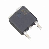
... December 2009 STF20NF20, STP20NF20 low gate charge STripFET™ Power MOSFET 110 110 W TO-220FP Figure 1. Marking Package 20NF20 DPAK 20NF20 TO-220FP 20NF20 TO-220 Doc ID 13154 Rev 4 STD20NF20 TO-220 3 1 DPAK Internal schematic diagram Packaging Tape and reel Tube Tube www.st.com 3 2 1/15 15 ...
Page 2
... Contents Contents 1 Electrical ratings . . . . . . . . . . . . . . . . . . . . . . . . . . . . . . . . . . . . . . . . . . . . 3 2 Electrical characteristics . . . . . . . . . . . . . . . . . . . . . . . . . . . . . . . . . . . . . 4 2.1 Electrical characteristics (curves) 3 Test circuits 4 Package mechanical data . . . . . . . . . . . . . . . . . . . . . . . . . . . . . . . . . . . . 10 5 Packaging mechanical data . . . . . . . . . . . . . . . . . . . . . . . . . . . . . . . . . . 13 6 Revision history . . . . . . . . . . . . . . . . . . . . . . . . . . . . . . . . . . . . . . . . . . . 14 2/ Doc ID 13154 Rev 4 STD20NF20, STF20NF20, STP20NF20 . . . . . . . . . . . . . . . . . . . . . . . . . . . . 6 ...
Page 3
... STD20NF20, STF20NF20, STP20NF20 1 Electrical ratings Table 2. Absolute maximum ratings Symbol V Drain-source voltage ( Gate- source voltage GS I Drain current (continuous Drain current (continuous (1) I Drain current (pulsed Total dissipation at T TOT Derating factor (2) dv/dt Peak diode recovery voltage slope Insulation withstand voltage (RMS) from all ...
Page 4
... ± Parameter Test conditions MHz 100 4.7 Ω (see Figure 15 160 (see Figure 16) Doc ID 13154 Rev 4 STD20NF20, STF20NF20, STP20NF20 Min. Typ 200 = 125 ° 250 µ 0.10 Min. Typ 940 - 197 5.6 14.5 Max. Unit V 1 µA 10 µA ±100 Ω 0.125 Max ...
Page 5
... STD20NF20, STF20NF20, STP20NF20 Table 7. Source drain diode Symbol Source-drain current I SD Source-drain current (1) I SDM (pulsed) (2) V Forward on voltage SD t Reverse recovery time rr Q Reverse recovery charge rr I Reverse recovery current RRM t Reverse recovery time rr Q Reverse recovery charge rr I Reverse recovery current RRM 1 ...
Page 6
... Electrical characteristics (curves) Figure 2. Safe operating area for TO-220, DPAK Figure 4. Safe operating area for TO-220FP Figure 6. Output characteristics 6/15 STD20NF20, STF20NF20, STP20NF20 Figure 3. Thermal impedance area for TO-220, DPAK Figure 5. Thermal impedance for TO-220FP Figure 7. Transfer characteristics Doc ID 13154 Rev 4 ...
Page 7
... STD20NF20, STF20NF20, STP20NF20 Figure 8. Transconductance Figure 10. Gate charge vs gate-source voltage Figure 11. Capacitance variations Figure 12. Normalized gate threshold voltage vs temperature V GS(th) (norm) 1.10 1.00 0.90 0.80 0.70 0.60 0.50 0.40 - Figure 9. AM03979v1 T =-50° =25° =175° (A) D Figure 13. Normalized on resistance vs ...
Page 8
... Electrical characteristics Figure 14. Source-drain diode forward characteristics V SD (V) T =-50°C J 0.9 0.8 0.7 0.6 0 8/15 AM03982v1 T =25° =175° ( Doc ID 13154 Rev 4 STD20NF20, STF20NF20, STP20NF20 ...
Page 9
... STD20NF20, STF20NF20, STP20NF20 3 Test circuits Figure 15. Switching times test circuit for resistive load D.U. Figure 17. Test circuit for inductive load switching and diode recovery times FAST L=100µH G D.U.T. DIODE Ω Figure 19. Unclamped inductive waveform Figure 16. Gate charge test circuit 3.3 2200 µ ...
Page 10
... Package mechanical data 4 Package mechanical data In order to meet environmental requirements, ST offers these devices in different grades of ® ECOPACK packages, depending on their level of environmental compliance. ECOPACK specifications, grade definitions and product status are available at: www.st.com. ECOPACK trademark. 10/15 STD20NF20, STF20NF20, STP20NF20 Doc ID 13154 Rev 4 ® ...
Page 11
... STD20NF20, STF20NF20, STP20NF20 TO-220 type A mechanical data Dim Min A 4.40 b 0.61 b1 1.14 c 0.48 D 15. 2.40 e1 4.95 F 1.23 H1 6. 3.50 L20 L30 ∅P 3.75 Q 2.65 Doc ID 13154 Rev 4 Package mechanical data mm Typ Max 4.60 0.88 1.70 0.70 15.75 1.27 10.40 2.70 5 ...
Page 12
... Package mechanical data DIM 12/15 STD20NF20, STF20NF20, STP20NF20 TO-252 (DPAK) mechanical data mm Doc ID 13154 Rev 0068772_G ...
Page 13
... STD20NF20, STF20NF20, STP20NF20 5 Packaging mechanical data DPAK FOOTPRINT All dimensions are in millimeters TAPE MECHANICAL DATA mm DIM. MIN. MAX. A0 6.8 B0 10.4 10.6 B1 12.1 D 1.5 D1 1.5 E 1.65 1.85 F 7.4 K0 2.55 2.75 P0 3.9 P1 7 15.7 16.3 TAPE AND REEL SHIPMENT inch MIN. MAX. ...
Page 14
... Revision history 6 Revision history Table 8. Revision history Date 25-Jan-2007 20-Mar-2007 27-Apr-2007 10-Dec-2009 14/15 Revision 1 First release 2 Typo mistake in first page (order codes) Table 6: Dynamic 3 Updates on 4 Modified device summary on first page Doc ID 13154 Rev 4 STD20NF20, STF20NF20, STP20NF20 Changes ...
Page 15
... STD20NF20, STF20NF20, STP20NF20 Information in this document is provided solely in connection with ST products. STMicroelectronics NV and its subsidiaries (“ST”) reserve the right to make changes, corrections, modifications or improvements, to this document, and the products and services described herein at any time, without notice. All ST products are sold pursuant to ST’s terms and conditions of sale. ...